Showing Spotlights 209 - 216 of 338 in category All (newest first):
 Molybdenum disulfide's (MoS2) semiconducting ability, strong light-matter interaction and similarity to the carbon-based graphene makes it of interest to scientists as a viable alternative to graphene in the manufacture of electronics, particularly photoelectronics. In particular, MoS2 has excellent optical properties when deposited as a single, atom-thick layer - unlike graphene, it emits light when excited; albeit relatively poorly. In order to realize the potential of atomically thin MoS2 as a nanoscale active material in a light source, a considerable enhancement of its emission efficiency is necessary.
Mar 12th, 2015
 Heat energy can be converted into electricity with very high efficiency through a temperature-induced electron flow process known as thermionic emission. Thermionic energy converters have been used with different heat sources, all of them requiring operation at high temperatures above 1500 K. A new study indicates that heat temperature can be lowered by an order of magnitude if using graphene as hot cathode. The findings indicate that a graphene-based cathode thermionic converter operating at 900 K could reach an efficiency of 45%.
Mar 5th, 2015
 In an effort to find a way to introduce folds or waves into graphene in a simple and large-scale way, researchers have invented a rubber-stamp printing method to introduce waves into the graphene. The ability to controllably form folds in graphene has significant research and technological applications. Induced folds have a sublithographic width and macroscopic length. They could be used as channel materials or interconnects in chips, and it has been shown that stable field emitters are formed by folded graphene.
Feb 16th, 2015
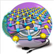
 The successful implementation of graphene-based devices invariably requires the precise patterning of graphene sheets at both the micrometer and nanometer scale. It appears that 3D-printing techniques are an attractive fabrication route towards three-dimensional graphene structures. Researchers have now used flakes of chemically modified graphene, namely graphene oxide GO and its reduced form rGO, together with very small amounts of a responsive polymer, to formulate water based ink or pastes to be used in 3D printers.
Feb 9th, 2015
 A comprehensive analysis of the fundamental properties, synthesis approaches and the future prospects of silicene, germanene, stanene, and phosphorene. It covers the literature on the fundamental properties of graphene analogous elemental sheets, inclusive of both theoretical and experimental knowledge. Various bottom-up synthesis techniques and top-down exfoliation approaches for the fabrication of two-dimensional elemental sheets are discussed.
Jan 21st, 2015
 Researchers have developed a simple method to thermally ablate highly resistant cancer cells using targeted biodegradable graphene nanoparticles. They found that graphene can convert non-ionizing radio waves - the same that are used in FM radios - into heat energy at microscopic levels. This heat is sufficient to completely destroy proteins and DNA inside individual cancer cells, irrespective of any kinds of resistant mechanisms that drives cancer cells at advanced stages.
Jan 16th, 2015
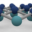
 Researchers have identified novel 2D wide-band-gap semiconductors with high stabilities, namely monolayer arsenene and antimonene. These materials are indirect wide-band-gap semiconductors, and under strain, they become direct band-gap semiconductors. For arsenene and antimonene, such dramatic transitions of electronic properties could open a new door for nanoscale transistors with high on/off ratio, blue/UV optoelectronic devices, and nanomechanical sensors based on new ultrathin semiconductors.
Jan 14th, 2015
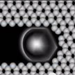 A widely discussed method for the patterning of graphene is the channelling of graphene by metal nanoparticles in oxidizing or reducing environments. Researchers have now performed in-situ transmission electron microscopy experiments of silver nanoparticles channeling on graphene and discover that the interactions in the one-dimensional particle-graphene contact line are sufficiently strong so as to dictate the three-dimensional shape of the nanoparticles.
Dec 19th, 2014
 Subscribe to our Nanotechnology Spotlight feed