Showing Spotlights 2297 - 2304 of 2785 in category All (newest first):
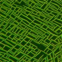
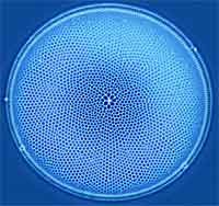 Diatoms are a major group of hard-shelled algae and one of the most common types of phytoplankton. A characteristic feature of diatom cells is that they are encased within a unique cell wall made of silica. Silicate materials are very important in nature and they are closely related to the evolution of living organisms. Diatom walls show a wide diversity in form, some quite beautiful and ornate, but usually consist of two symmetrical sides with a split between them, hence the group name. There is great potential for the use of diatoms in nanotechnology. This potential lies in the pores and channels which give rise to a greatly increased surface area, and the silica structure which lends itself to chemical modification. In addition there is a huge variety in the sizes and shapes of diatoms available, providing scope for the selection of a particular species of diatom tailored to a particular requirement. Researchers in the UK have demonstrated that the silica walls of diatoms can be used for the attachment of active biomolecules, such as antibodies, using either primary amine groups or the carbohydrate moiety. These modified structures can, therefore, be used for antibody arrays or for use in techniques such as immunoprecipitation.
Feb 7th, 2008
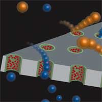 Nanopores function as membrane channels in all living systems, where they serve as sensitive electro-mechanical devices that regulate electrical potential, ionic flow, and molecular transport through the cell membrane. Scientists are studying nanopore construction with the goal of making man-made cell membranes and single molecule detectors. So far, nanoporous membrane-based separations simply use the difference in size of the analytes relative to pore size in the membrane. Here, for a nanopore to be useful as a single molecule detector, its diameter must not be much larger than the size of the molecule to be detected. When a single molecule enters a nanopore in an insulating membrane, it causes changes in the nanopore's electrical properties, which then can be detected and measured. In order to bring about selectivity beyond size, it is necessary that methods for functionalizing the membrane pores are available. To that end, researchers have developed a very simple, but versatile, method for decorating the nanoporous membranes with functional groups. By uniformly modifying the internal cavities of nanopores with various polymers they were able to demonstrate selectivities based on size, charge and hydrophobicity of the molecule passing through the nanopore.
Feb 6th, 2008
 Walk into an intensive care unit and you're likely to see many of the patients sporting a 'central line' - a plastic tube placed in a large vein that goes to the heart. A central line is a very efficient way to pump nutrients, antibiotics or other drugs directly into the bloodstream. Unfortunately it is also a cause for bloodstream infections (sepsis) and central lines remain an important cause for hospital deaths. An estimated 200,000 bloodstream infections occur each year in the U.S. alone, the majority associated with the presence of an intravascular catheter. The Institute for Healthcare Improvement (IHI) estimates the yearly death toll from blood infections related to intravenous lines to be as high as 28,000. Numerous pathogens can cause sepsis and the death toll could be reduced if the specific pathogen could be identified more quickly than it is usually done today using blood cultures (the laboratory examination of a blood sample to detect the presence of disease-causing microorganisms). One solution would be to determine the pathogen's DNA, requiring a rapid DNA assay with the potential for mutant identification and multiplexing. Current DNA assays are based on thermal dehybridization or melting of the DNA duplex helix - the melting temperature of DNA is determined by its base sequence - a process that can take up to an hour. Researchers in Germany have developed a novel technique that allows for DNA analysis in the millisecond range. Their method has great potential to vastly improve the speed of pathogen detection.
Feb 5th, 2008
 More and more carbon nanotube (CNT) applications are moving from the research lab into commercial products. For example, CNTs can be found already in tennis rackets and bicycles, displays and TV screens, and numerous resins used by aerospace, defense, health care, and electronics companies. Not surprisingly, CNT production is growing by hundreds of metric tons a year. One of the large suppliers alone, Bayer, is talking about having 3,000 metric tons of production capacity in place by 2012. As a result of the increasing supply, prices are dropping fast. While a kilogram of multi-walled CNTs (MWCNTs) sold for tens of thousands of dollars just a few years ago (and single-walled CNTs still do), the price for some types of MWCNTs has fallen to hundreds of dollars per kg. Recent market analyses forecast sales of all nanotubes to reach $1 billion to $2 billion annually within the next four to seven years. In terms of dollar value, electronics devices will be the largest end-use category, although composite materials in automotive applications may account for greater volumes. These volumes are expected to approach several thousand metric tons per year. This means that the exposure to CNTs, especially by factory workers, will increase substantially over the next few years. Since the jury is still out as to the toxicity of nanotubes it appears prudent to at least develop suitable sensor technology to detect CNTs, especially in the workplace.
Feb 4th, 2008
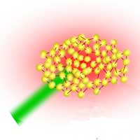
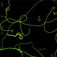
 The vision of revolutionary bottom-up nanotechnology is based on a concept of molecular assembly technologies where nanoscale materials and structures self-assemble to microscale structures and finally to macroscopic devices and products. We are a long way from realizing this vision but researchers are busily laying the foundation for nanoscale engineering. Assembling nanoscopic components into macroscopic materials is an appealing goal but one of the enormous difficulties lies in bridging approximately six orders of magnitude that separate the nanoscale from the macroscopic world. Until machinery capable of automated and industrial-scale nano-assembly can be built, the parallelism of chemical synthesis and self-assembly is necessary when controlling materials at the nanoscale. An obvious direct approach to molecular nanotechnology therefore is to start with organic molecules as building blocks. Modest from the viewpoint of molecular manufacturing visionaries, but quite fascinating to a lot of scientists, research into nanofibers, as a modification of organic crystals, is making good progress. New research results coming out of Denmark offer the basis for a novel organic-molecule-based nanotechnological concept that allows for a multitude of applications in fundamental research and in device applications. Essentially, this concept is based on three steps: 1) directed self-assembled surface growth of nanofibers from functionalized molecules; 2) transfer and manipulation of individual fibers as well as of ordered arrays; and 3) device integration.
Feb 1st, 2008
 'Smart' is the key buzz word used by materials engineers when they describe the future of coatings, textiles, building structures, vehicles and just any material that you can think of. Materials are made 'smart' when they are engineered to have properties that change in a controlled manner under the influence of external stimuli such as mechanical stress, temperature, humidity, electric charge, magnetic fields etc. Nature of course is full with 'smart' materials that are capable of adapting to new tasks, are self-healing, and can self-assemble autonomously simply out of a solution of building blocks. Duplicating this feat with man-made materials will one day become a reality thanks to nanotechnology. Scientists not only dream about self-repairing cars or building walls that turn transparent like windows, they are actively working on the first steps towards these goals. Simple smart materials (that are not nanotechnology based) are already a reality, such as piezoelectric materials and shape memory alloys. Emerging nanotechnologies are now about to give scientists the tools to take smart materials to the next performance level. For instance, the European project Inteltex is developing a new, multifunctional textile that could be used as a wallpaper to detect temperature changes or chemical leakage or that could be used in medical and protective wear to monitor body temperature and mechanical stress. MIT's Institute for Soldier Nanotechnologies works on smart surfaces that switch properties. Nanotechnology-enabled smart materials are still very early days but basic progress is being made. Another small building block towards smart materials was recently reported by Italian researchers who demonstrated photo-switchable nanofibers based on the reversible transformation between two molecular photochemical states, exhibiting different chemico-physical characteristics.
Jan 31st, 2008
 Our sense of touch connects us to the world around us and is an integral part of how we experience things, both physically and emotionally. In the virtual world of remote-control robots, scientific models or computer games, users generally lack tactile, or haptic (from the Greek word Haphe, pertaining to the sense of touch), feedback, which either makes delicate manipulative tasks difficult or keeps the subject purely visual and often inscrutable (an electron microscope image of a nanoscale object, for instance). The desire for natural and intuitive human machine interaction has led to the inclusion of haptics in man-machine interfaces. The user is able to control inputs to the system through hand movements and in turn receives feedback through tactile stimulation in the hands. Sophisticated, state-of-the-art haptic user-interface software is capable of adding interactive, realistic virtual touch capabilities to human-computer interactions. Among the uses are medical applications, remote vehicle or robotic control, military applications, and video games. Users are said to feel realistic weight, shape, texture, dimension, dynamics, and force effects. Applying the use of real-time virtual reality and multisensory user interface to nanoscience, scientists in France have begun to open up the otherwise only scientifically described reality of the nanoworld to a non-scientific public.
Jan 30th, 2008
 When the U.S. enacted its 21st Century Nanotechnology Research and Development Act in 2003 it was clearly understood that the impact of nanotechnologies on all aspects of society would be deeply transformational. As the National Nanotechnology Initiative was set up, its goals were not only defined as 'maintaining a world-class research and development program aimed at realizing the full potential of nanotechnology' but also to 'facilitate transfer of new technologies into products for economic growth, jobs, and other public benefit'. The first part regarding world-class R&D is happening. The second part, converting the research and development results into economic growth and jobs, is nowhere to be seen yet.
Jan 29th, 2008
 Subscribe to our Nanotechnology Spotlight feed