Nanotechnology Spotlight – Latest Articles
 Subscribe to our Nanotechnology Spotlight feed
Showing Spotlights 2289 - 2296 of 3575 in category All (newest first):

Converting eggshell membranes into a high-performance electrode material for supercapacitors
Ultra- or supercapacitors are emerging as a key enabling storage technology for use in fuel-efficient transport as well as in renewable energy. These devices combine the advantages of conventional capacitors - they can rapidly deliver high current densities on demand - and batteries - they can store a large amount of electrical energy. Today's commercial supercapacitors store energy in two closely spaced layers with opposing charges and offer fast charge/discharge rates and the ability to sustain millions of cycles. Researchers have come up with various electrode materials to improve the performance of supercapacitors, focussing mostly on porous carbon due to its high surface areas, tunable structures, good conductivities, and low cost. In recent years, this has increasingly included research on various carbon nanomaterials such as carbon nanotubes, carbon nano-onions, or graphene. In new work, researchers have demonstrated that a common daily waste - the eggshell membrane - can be converted into a high-performance carbon material for supercapacitors.
April 12, 2012

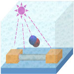
Solar-powered cement production without carbon dioxide emissions
The global cement industry is currently one of the largest single emitter of carbon dioxide, generating on average about 830 kg of this greenhouse gas for each 1000 kg of cement produced. Considering that the worldwide annual production of cement is a whopping 3.8 trillion kg, the cement industry alone accounts for approximately 5-6% of man-made CO2 emissions. Researchers have now presented a solar-powered process to produce cement without any carbon dioxide. In their STEP (Solar Thermal Electrochemical Production) process, cement limestone undergoes low energy electrolysis to produce lime, O2 and reduced carbonate without carbon dioxide emission. In this new technique, the kiln limestone-to-lime process is replaced by an electrolysis process which changes the product of the reaction of the limestone as it is converted to lime.
April 11, 2012
UV light illuminates the tremendous sensing potential of single-walled carbon nanotubes
Single-walled carbon nanotubes arguably are the ultimate biosensor among nanoscale semiconducting materials due to their high surface-to-volume ratio and unique electronic structure. After more than a decade of excitement though, more and more researchers in the nanotube field believe that pristine SWCNTs are very limited as a sensing material. Ironically the ultrahigh sensitivity of SWCNTs is easily compromised by various unintentional contaminants from the device fabrication process as well as the ambient environment. As a result, significant efforts have been focused on all kinds of ways to functionalize or decorate nanotubes with other species in order to improve their sensitivity. Researchers have now shown that applying continuous in situ ultraviolet light illumination during gas detection can enhance a SWCNT-sensor's performance by orders of magnitude under otherwise identical sensing conditions.
April 10, 2012
Novel functional nanoarchitectures based on nanotube-bridged wires
On-wire lithography is a recently developed nanotechnology fabrication technique that allows researchers to synthesize billions of gapped nanowires with nanometer control of gap length, within a single experiment. These gaps can then be used to integrate different material segments into a single nanowire in order to fabricate functional devices. In recent work, researchers have reported a simple but efficient method to use OWL to mass produce nanotube-bridged nanowires, including carbon nanotube (CNT) channels with channel lengths as small as 5 nm. Since the CNT-bridged nanowires are comprised of CNT junctions with gold electrodes, each of the nanowires could for instance work as a CNT-based sensing device, ballistic transistors, or resonators.
April 5, 2012

Controlling the diffraction of light by using light
All-optical processes could allow dramatic speed increase in photonics by eliminating the need to convert photonic signals to electronic signals and back for switching. The many opportunities that all-optical processes could bring to photonics have been hampered by the lack of materials that combined photosensitivity with fast, large, and reversible changes in their optical properties at the influence of light. By exploited the universal capabilities of an 'active polymeric template' for confining, orienting, and stabilizing a wide range of self-organized materials, researchers recently have exploited a wide range of optical, electro-optical and all-optical effects which confirm the extraordinary capability of their 'active polymeric template' to induce self-organization, without using any kind of surface chemistry or functionalization.
April 4, 2012
Researchers succeed in achieving high-contrast superlens lithography
The concept of a 'superlens' has attracted significant research interest in the imaging and photolithography fields since the concept was proposed back in 2000. A superlens would allow you to view objects much smaller than the roughly 200 nanometers that a regular optical lens with visible light would permit. Since superlenses have demonstrated the capability of subdiffraction-limit imaging, they have been envisioned as a promising technology for potential nanophotolithography. Unfortunately, all the experimentally demonstrated photoresist patterns exhibited very low profile depths, leading to poor contrasts, which are far below industrial requirements. Researchers have now experimentally demonstrated sub-50 nm resolution nanophotolithography by using a smooth silver superlens under 365 nm UV light in a conventional photolithography setup.
April 3, 2012
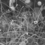
Calcium silicate as a metal-free catalyst for carbon nanotube synthesis
Of all the methods that have been developed to produce carbon nanotubes (CNTs), including arc discharge, laser ablation, and chemical vapor deposition (CVD), CVD is the most technically important and the most widely used in industry. Using the CVD process, manufacturers can combine a metal catalyst such as iron or nickel with reaction gases such as hydrocarbon to form carbon nanotubes inside a high-temperature furnace. Semiconductor nanoparticles such as silicon carbide, germanium and silicon have also been used for single CNT catalysis. However, these catalyst materials are usually expensive and need to be of high purity in order to be useful for the growth of carbon nanotubes. Researchers have now found that cheap and plentiful calcium silicate can absorb carbon species and grow multi-walled carbon nanotubes.
April 2, 2012

Graphene nanosensor tattoo on teeth monitors bacteria in your mouth
Early detection of pathogenic bacteria is critical to prevent disease outbreaks and preserve public health. This has led to urgent demands to develop highly efficient strategies for isolating and detecting this microorganism in connection to food safety, medical diagnostics, water quality, and counter-terrorism. A team of scientists has now developed a novel approach to interfacing passive, wireless graphene nanosensors onto biomaterials via silk bioresorption. The nanoscale nature of graphene allows for high adhesive conformality after biotransfer and highly sensitive detection. The team demonstrates their nanosensor by attaching it to a tooth for battery-free, remote monitoring of respiration and bacteria detection in saliva.
March 29, 2012