Nanotechnology Spotlight – Latest Articles
 Subscribe to our Nanotechnology Spotlight feed
Showing Spotlights 2281 - 2288 of 3575 in category All (newest first):

Nanotechnologies from the consumers' point of view - the hype appears to be fading
The study focused on the following questions: What do consumers know about nanotechnologies? How do they rate nanotechnologies? How do they obtain information? How would they like to be informed in the future? The results show that the "Nano-Hype" appears to be fading. Surprisingly, regarding the quality of the consumers' statements, e.g. how detailed their descriptions of the individual examples are, it can be said that their knowledge about all fields of application has decreased. Even though the knowledge about all fields of application has decreased, particularly striking is the decline in the fields of surface coatings, construction materials and environmental engineering. In sum, it can be hypothesised that consumer communication on the part of product manufacturers has decreased considerably, or that the information does not reach the target group to the same extent. The public knowledge on nanotechnologies has become more abstract.
May 2, 2012

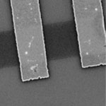
High-performing supercapacitor electrodes made from self-organizing cobalt oxide nanowires
Commercially available supercapacitors store energy in two closely spaced layers with opposing charges and offer fast charge/discharge rates and the ability to sustain millions of cycles. Researchers have come up with various electrode materials to improve the performance of supercapacitors, focussing mostly on porous carbon due to its high surface areas, tunable structures, good conductivities, and low cost. Researchers at KAUST now have developed novel supercapacitor electrodes with remarkable pseudocapacitance. They used a scheme of current collector dependent self-organization of mesoporous cobalt oxide nanowires has been used to create unique supercapacitor electrodes, with each nanowire making direct contact with the current collector.
April 30, 2012
Selective gas sensing with pristine graphene
It has been known for some time that graphene can be used for detection of individual gas molecules adsorbed on its surface - a graphene sensor can detect just a single molecule of a toxic gas. However, the extremely high sensitivity of graphene does not necessarily translate into its selectivity to various molecules. In other words, it can be detected that some molecules attached to the graphene surface change the resistivity of a graphene field-effect transistor but one cannot say what kind of a molecules have attached. Scientists have therefore thought that truly selective gas sensing with graphene devices requires the functionalization of graphene surface with some agents specific for different gas molecules. In new research, though, scientists have now found that chemical vapors change the noise spectra of graphene transistors. The noise signal for each gas is reproducible, opening the way for practical reliable and simple gas sensors made from graphene.
April 26, 2012

Thermoelectric nanocomposites switch between heat and electricity in a unique and clean solid-state approach
In the past couple of decades, thermoelectrics have been drawing more and more research interest due to the limited availability and the negative environmental impact of conventional energy strategies. In the past, as a measuring stick of the conversion efficiency, the term "dimensionless figure-of-merit," also referred to as ZT, has been widely used. A high ZT value usually promises high thermoelectric performance. Typically, good thermoelectric materials should simultaneously display low thermal conductivity and good electrical conductivity. Striving to enhance the performance of thermoelectric materials, researchers from Boston College and MIT have recently reported a novel materials design to achieve a 30 to 40% enhancement in the peak ZT value for n-type SiGe semiconducting alloys.
April 25, 2012
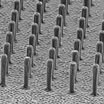
Novel electrochemical sensing platform based on graphene encrusted 3D microstructures
Graphene with its distinctive band structure and unique physiochemical properties - such as exceptionally low intrinsic electrical resistivity, high surface area, rapid electrode kinetics and good mechanical properties - is considered an attractive material for analytical electrochemistry. However, one of the key technical challenges for the use of graphene as functional material in device applications is the integration of nanoscale graphene onto micro- or millimeter sized sensing platforms. With a new methodology, a team from Florida International University was able to integrate graphene onto three-dimensional (3D) carbon microstructure arrays with good uniformity and controllable morphology.
April 24, 2012

Improving banknote security with organic electronics
Counterfeiting of bank notes has always been a problem and central banks are leading a high-tech fight against sophisticated counterfeiting operations. For instance, when the European Central Bank designed its new banknotes, they included a variety of security features - holograms, foil stripes, special threads, microprinting, special inks and watermarks. Another high-tech approach are imprinting radio frequency identification (RFID) tags onto banknotes. While the integration of RFID technology on a banknote is technically possible, no banknotes in the world today employ such a technology. In recent work, researchers in Saudi Arabia have now fabricated the first-ever all-polymer, non-volatile, ferroelectric memory on banknotes.
April 23, 2012
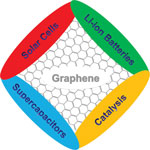
Graphene-based nanotechnology in energy applications
Graphene-based materials are emerging as highly attractive materials for real applications, especially in the area of energy conversion and storage. There are four major energy-related areas where graphene will have an impact: solar cells, supercapacitors, lithium-ion batteries, and catalysis for fuel cells. A recent review gives a brief overview of the recent research concerning chemical and thermal approaches toward the production of well-defined graphene-based nanomaterials and their applications in energy-related areas. But before graphene-based nanomaterials and devices find widespread commercial use, two important problems have to be solved: one is the preparation of graphene-based nanomaterials with well-defined structures, and the other is the controllable fabrication of these materials into functional devices.
April 18, 2012

Nanotechnology for development
In recent years billions of dollars have been invested in nanotechnology research. Nanotechnology is said to have such pervasive consequences that the 21st century is already proclaimed to become the 'nano-century'. Nanotechnology may also contribute to development in the global South. The new characteristics of nanotechnologies are also said to offer solutions for problems faced by people in the global South, especially in the fields of water, energy, and health. For instance water filters, energy storage systems, solar powered electricity and portable diagnostic tests may be developed and improved using nanotechnology. But the very same features that give rise to new opportunities may also generate new risks. There may be risks to the human body and environment. But for instance also investing in nanotechnology itself can be seen as a risk.
April 17, 2012