Nanotechnology Spotlight – Latest Articles
 Subscribe to our Nanotechnology Spotlight feed
Showing Spotlights 2353 - 2360 of 3575 in category All (newest first):
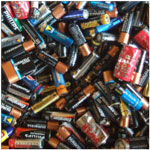
Nanotechnology could make battery recycling economically attractive
Many batteries still contain heavy metals such as mercury, lead, cadmium, and nickel, which can contaminate the environment and pose a potential threat to human health when batteries are improperly disposed of. Not only do the billions upon billions of batteries in landfills pose an environmental problem, they also are a complete waste of a potential and cheap raw material. Unfortunately, current recycling methods for many battery types, especially the small consumer type ones, don't make sense from an economical point of view since the recycling costs exceed the recoverable metals value. Researchers in India have carried out research to address the recycling of consumer-type batteries. They report the recovery of pure zinc oxide nanoparticles from spent Zn-Mn dry alkaline batteries.
December 1, 2011
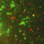
A fast nanotechnology platform to detect/capture bacteria in clinical samples
Surface-enhanced Raman spectroscopy (SERS) is a powerful research tool that is being used to detect and analyze chemicals as well as a non-invasive tool for imaging cells and detecting cancer. It also has been employed for label-free sensing of bacteria, exploiting its tremendous enhancement in the Raman signal. SERS can provide the vibrational spectrum of the molecules on the cell wall of a single bacterium in a few seconds. Such a spectrum is like the fingerprints of the molecules and therefore could be exploited as a means to quickly identify bacteria without the need of a time-consuming bacteria culture process, which typically takes a few days to several weeks depending on the species of bacteria. To practically apply SERS to the early diagnosis of bacteremia - the presence of bacteria in the blood - researchers have managed to capture bacteria in a patient's blood onto the SERS substrate.
November 29, 2011
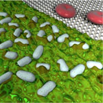
Catch and release sensing of single malaria-infected red blood cells
Graphene research papers are popping up left and right at what seems like an accelerating speed and growing volume. One of the areas that is seeing vast research interest is the biological interfacing of graphene for instance for sensor applications. Today, we are looking at another exciting graphene bio application where a graphene sensor is integrated with microfluidics to sense malaria-infected red blood cells at the single-cell level. Specific binding between ligands on positively charged knobs of infected red blood cells and receptors functionalized on graphene inside microfluidic channels induces a distinct conductance change. Conductance returns to baseline value when infected cell exits the graphene channel.
November 28, 2011

Natural nanomaterials - they are everywhere
Naturally occurring nanomaterials can be found everywhere in nature and only with recent advances in instrumentation and metrology equipment are researchers beginning to locate, isolate, characterize and classify the vast range of their structural and chemical varieties. Scientists are beginning to recognize that all sources of nanomaterials are important in evaluating the possible impact of nanoscale materials on human health and the environment; however, perhaps the greatest benefit to studying these materials will be in their ability to inform researchers about the manner in which nano-sized materials have been a part of our environment from the beginning.
November 24, 2011
Eavesdropping on cells with graphene transistors
The integration of biological components with electronics, and more specifically, the interfacing of complex biological systems is one of the current challenges on the path towards bioelectronics (or bionics for short). Up to know, and due to its technology maturity, most of the work has been done based on Si-FET technology. However, there have been some issues related to this technology which prevented a more successful implementation into real applications. Researchers have now demonstrated, for the first time, that CVD grown graphene can be employed to fabricate arrays of transistors which are able to detect the electrical activity of electrogenic cells.
November 22, 2011
A new tool to track the intracellular trafficking of nanomedicines
In nanomedicine, nanoparticles are used as vehicles for efficiently delivering therapeutic nucleic acids, such as disease-fighting genes and small interfering RNA (siRNA) molecules, into cells. But getting nanomedicines to their target sites inside cells is not the only challenge. It also is necessary to assess the intracellular processing of nanomedicines and the efficacy of their payload delivery - a task that is not exactly trivial given the complexity and dynamics of the mechanisms of endocytosis and intracellular trafficking. Researchers are therefore trying to develop robust and reliable tools to characterize and evaluate the intracellular processing of administered nanomedicines. As part of this effort, scientists have now introduced a quantitative approach to study live-cell endosomal colocalization dynamics of nanomedicines for gene delivery, based on single-particle tracking and trajectory-correlation.
November 21, 2011
Non-toxic, solution-based inorganic solar cell chemistry with Earth-abundant elements
While the current solar panel market is still dominated by crystalline silicon solar cells, thin-film solar cell technologies based on chalcogenides are dramatically increasing their market penetration. Apart from device performance, price volatility issues, rare earth elements scarcity issues, and potential environmental issues have raised some concerns about both CdTe and CIGS. A frontrunner in the search for the next generation of thin film photovoltaic materials are low-cost quaternary copper-zinc-tin-sulfide (CZTS) and copper-zinc-tin-chalcogenide (CZTSSe). Notably, these materials are composed of naturally abundant elements in the Earth's crust and have very low toxicity. New research show that there are other chemical routes that use much more benign solvents by demonstrating a simple and facile solution phase method to form CZTS thin film solar cell using commercially available precursors and non-toxic solvents with high yield.
November 18, 2011
Breakthrough allows rapid, CMOS-compatible fabrication of large 3D photonic crystals
There is a lot of buzz in the computer industry about so-called three-dimensional (3D) chips, promising higher performance with lower energy consumption, and paving the way for exascale computers (which would represent a thousandfold increase in performance over the current petascale architecture). However, these chips are not intrinsically built, true 3D chips; rather, they are stacked layers of up to 100 separate chips. In a major breakthrough in the field of photonic crystals, researchers in The Netherlands have developed a novel process that allows for rapid fabrication of large 3D photonic crystals in mono-crystalline silicon using CMOS compatible processes.
November 17, 2011