Nanotechnology Spotlight – Latest Articles
 Subscribe to our Nanotechnology Spotlight feed
Showing Spotlights 2345 - 2352 of 3575 in category All (newest first):
Lesson from nature greatly strengthens the potential of block copolymer lithography
Block copolymer lithography is a cost-effective, parallel, and scalable nanolithography for the densely packed periodic arrays of nanoscale features, whose typical dimension scale is beyond the resolution limit of conventional photolithography. So far, it has been impossible to utilize block copolymer lithography on low surface energy materials such as Teflon, graphene or gold, where block copolymer thin film generally de-wets. To address this technological challenge, researchers in South Korea introduced block copolymer lithography that employs polydopamine coating - inspired by the adhesive proteins secreted by mussels - as a surface pretreatment for universal wettability generally applicable to arbitrary surfaces.
December 15, 2011

Fighting Alzheimer's disease with nanotechnology
Alzheimer's disease is among the most common brain disorders affecting the elderly population the world over, and is projected to become a major health problem with grave socio-economic implications in the coming decades. The total number of people afflicted by Alzheimer's disease (AD) worldwide today is about 15 million people, a number expected to grow by four times by 2050. This review looks at some of the nanotechnology-enabled approaches that are being developed for early detection and accurate diagnosis of Alzheimer's, its therapeutic treatment, and prevention. These potential solutions offered by nanotechnology exemplify the growing significance that it holds for dealing with brain ailments in general.
December 13, 2011
Nanofabrication made easy with cheap, homemade benchtop photolithography system
Currently, the primary tool for defining patterns at the micro- and nanometer scale is the mask aligner. Even where soft lithography methods are used, mask aligners are still often required to fabricate the masters. A mask aligner is a machine that is bulky in size and weight and is limited in the area that it can pattern in a single step. Also, a significant amount of infrastructure is needed for operation, such as high voltage power supplies and gas cooling lines. The average cost of this tool is in the six figures, which is a barrier for many labs and businesses in research and development of nanotechnologies. Researchers have now developed a compact and portable photolithography system based on a solid-state light source to remove these limiting factors and, at the same time, make available the high quality patterns that a mask aligner can produce.
December 12, 2011

Nanotechnology and microbiology
Microbiology relates to nanoscience at a number of levels. Many bacterial entities are nano-machines in nature, including molecular motors like flagella and pili. Bacteria also form biofilms by the process of self-assembly. The formation of aerial hyphae by bacteria and fungi is also directed by the controlled and ordered assembly of building blocks. Also, the formation of virus capsids is a classical process of molecular recognition and self-assembly at the nanoscale. Nanoscience does have an impact on several areas of microbiology. It allows for the study and visualization at the molecular-assembly levels of a process. It facilitates identification of molecular recognition and self-assembly motifs as well as the assessment of these processes.
December 9, 2011

Self-propelled microrockets detect dangerous bacteria in food, clinical and environmental samples
Early detection of food borne pathogenic bacteria is critical to prevent disease outbreaks and preserve public health. This has led to urgent demands to develop highly efficient strategies for isolating and detecting this microorganism in connection to food safety, medical diagnostics, water quality, and counter-terrorism. Conventional techniques to detect E. coli and other pathogenic bacteria are time-consuming, labor-intensive, and inadequate as they lack the ability to detect bacteria in real time. Thus, there is an urgent need for alternative platforms for the rapid, sensitive, reliable and simple isolation and detection pathogens. Taking a novel approach to isolating pathogenic bacteria from complex clinical, environmental and food samples, researchers have developed a nanomotor strategy that involves the movement of lectin-functionalized microengines. Receptor-functionalized nanoswimmers offer direct and rapid target isolation from raw biological samples without preparatory and washing steps.
December 8, 2011
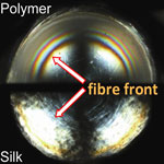
Spinning like the spider could cut energy cost of synthetic polymer fibers by 90%
Researchers have, for the first time, compared the energetic cost of silk and synthetic polymer fiber formation and demonstrated that, if we can learn how to spin like the spider, we should be able to cut the energy costs for polymer fiber processing by 90%, leaving alone the heat treatment requirements. The two routes of polymer fiber-spinning - one developed by nature and the other developed by man - show striking similarities: both start with liquid feed-stocks sharing comparable flow properties; in both cases the 'melts' are extruded through convergent dye designs; and for both 'spinning' results in highly ordered semicrystalline fibrous structures. In other words, analogous to the industrial melt spinning of a synthetic polymer, in the natural spinning of a silk the molecules (proteins) align (refold), nucleate (denature) and crystallize (aggregate).
December 7, 2011
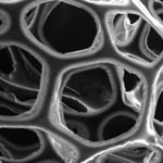
Carbon nanotube-coated sponge makes an excellent supercapacitor
Ultra- or supercapacitors are emerging as a key enabling storage technology for use in fuel-efficient transport as well as in renewable energy. These devices combine the advantages of conventional capacitors - they can rapidly deliver high current densities on demand - and batteries - they can store a large amount of electrical energy. Supercapacitors offer a low-cost alternative source of energy to replace rechargeable batteries. Although the energy density of capacitors is quite low compared to batteries, their power density is much higher, allowing them to provide bursts of electric energy. Researchers have now fabricated novel high-performance sponge supercapacitors using a simple and scalable method. Their results shows that three-dimensional electrodes potentially have a huge advantage over conventional mixed electrode materials.
December 6, 2011

Novel nanoimprint technique offers a low-cost route toward sub-10 nm nanopatterning
Directed self-assembly of block copolymers is a candidate lithography for use in future nanoelectronics and patterned media copolymer with resolutions down to the sub-10nm domain. Variations of this effective nanofabrication technique have been used to write periodic arrays of nanoscale features into substrates at exceptionally high densities with resolutions that are difficult or impossible to achieve with top-down techniques alone. However, in many cases these approaches are either too costly or too complex due to the required number of processing steps, for instance expensive, time-consuming substrate pre-patterning. Researchers at the Molecular Foundry have now shown that block copolymers can be aligned on an unpatterned substrate using a removable and reusable mold applied from above.
December 5, 2011