| Posted: Dec 05, 2011 |
Novel nanoimprint technique offers a low-cost route toward sub-10 nm nanopatterning |
| (Nanowerk Spotlight) Directed self-assembly of block copolymers is a candidate lithography for use in future nanoelectronics and patterned media copolymer with resolutions down to the sub-10nm domain. Variations of this effective nanofabrication technique have been used to write periodic arrays of nanoscale features into substrates at exceptionally high densities with resolutions that are difficult or impossible to achieve with top-down techniques alone. However, in many cases these approaches are either too costly or too complex due to the required number of processing steps, for instance expensive, time-consuming substrate pre-patterning. |
| "Directed self-assembly of block copolymers via nanoimprint has been a largely underexplored area in nanofabrication in part due to mold release issues," Deirdre Olynick, Ph.D., a Staff Scientist at the Molecular Foundry at the Berkeley Lab, explains to Nanowerk. The Molecular Foundry is one of five U.S. Department of Energy (DOE) Nanoscale Science Research Centers, national user facilities for interdisciplinary research at the nanoscale, supported by the DOE Office of Science. |
| "Mold release in nanoimprint technology persists as a significant obstacle to achieving reliable, high-quality patterning at the nanoscale," says Brett Helms, also a staff scientist at the Molecular Foundry. "Owing to the inherent high surface area contact between the mold and the imprinted film, the interfacial adhesion is often too high for efficient release, leaving behind damaged, deformed, or delaminated features and sullying the mold." |
| Reporting their findings in a recent edition of ACS Nano ("Sub-10 nm Nanofabrication via Nanoimprint Directed Self-Assembly of Block Copolymers"), the team led by Olynick and Helms, with former post-doc Sang-Min Park (now at Seagate), have now shown that block copolymers can be aligned on an unpatterned substrate using a removable and reusable mold applied from above. Alignment is achieved quickly due to flow induced by the nanoimprinting process. |
| Using thermal nanoimprint lithography for the directed self-assembly of block copolymers, the team was able to avoid any type of substrate prepatterning. This fabrication method is also particularly suited to the types of highly planar surfaces found in integrated circuit and magnetic media production. |
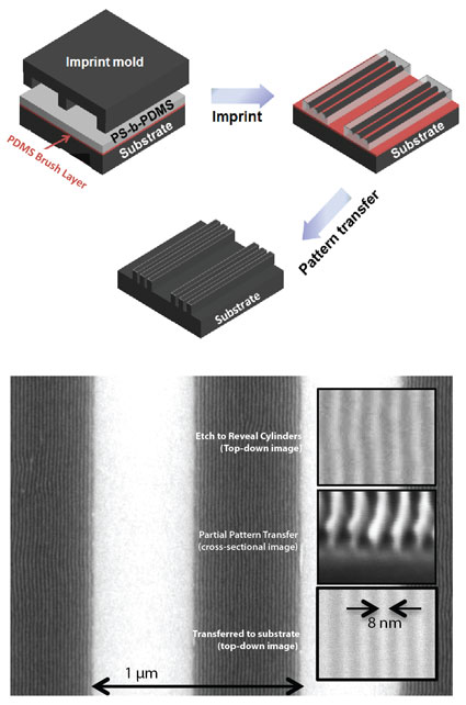 |
| Schematic of process (top). Micrographs of imprinted BCP and etch transfer to silicon dioxide. (Image: Dr. Olynick, The Molecular Foundry) |
| In previous work published earlier this year ("Interface Segregating Fluoralkyl-Modified Polymers for High-Fidelity Block Copolymer Nanoimprint Lithography"), the Molecular Foundry team already addressed the challenge of mold release during nanoimprint for directed self-assembly of block copolymers by using interface segregating surfactants which reduced block copolymers interfacial adhesion following thermal nanoimprint. |
| With regard to its potential for high-throughput processing, however, this technique had its limitations due to the need for a surface treatment of the mold inbetween imprints. |
| "Aiming to further advance the technique for high-throughput processing and pattern transfer, we investigated PDMS, polystyrene, and fluoroalkylsilane mold treatments toward reusable molds that do not require interface segregating surfactants," Olynick describes the idea behind the team's current work. |
| They found that grafting PDMS brushes onto the surface of imprint molds provided for good mold-release. |
| "Notably" Olynick points out, "PDMS was not the lowest interfacial energy treatment, yet it conferred the best results likely due to effects such as lower friction during release." |
| To demonstrate the effectiveness of their technique, the researchers achieved high quality patterns with a 25:1 density multiplication by using molds that can be generated with relatively low-cost optical lithography. Thus, starting from a much lower resolution, they managed to achieve ordered sub-10 nm features. They then went on to transfer the such achieved patterns of single-digit nanometer features to underlying silicon oxide using plasma etching. |
| "Our results show that direct patterning of block copolymers using nanoimprint offers a low-cost route toward high-resolution, single-digit nanopatterning for application in plasmonics, optoelectronics, and next-generation nanoelectronics," Olynick summarizes her team's results. " For instance, we are creating unique nanoelectronic devices by patterning graphene nanoribbons. By patterning at this length scale, we can take advantage of quantum effects in the material." |
| The team's future research will address means to create more complex patterns. The biggest challenge will be to control defects in the pattern. |
 By
Michael
Berger
– Michael is author of four books by the Royal Society of Chemistry:
Nano-Society: Pushing the Boundaries of Technology (2009),
Nanotechnology: The Future is Tiny (2016),
Nanoengineering: The Skills and Tools Making Technology Invisible (2019), and
Waste not! How Nanotechnologies Can Increase Efficiencies Throughout Society (2025)
Copyright ©
Nanowerk LLC
By
Michael
Berger
– Michael is author of four books by the Royal Society of Chemistry:
Nano-Society: Pushing the Boundaries of Technology (2009),
Nanotechnology: The Future is Tiny (2016),
Nanoengineering: The Skills and Tools Making Technology Invisible (2019), and
Waste not! How Nanotechnologies Can Increase Efficiencies Throughout Society (2025)
Copyright ©
Nanowerk LLC
|

Become a Spotlight guest author! Join our large and growing group of guest contributors. Have you just published a scientific paper or have other exciting developments to share with the nanotechnology community? Here is how to publish on nanowerk.com. |
