Nanotechnology Spotlight – Latest Articles
 Subscribe to our Nanotechnology Spotlight feed
Showing Spotlights 2369 - 2376 of 3575 in category All (newest first):

Graphene membranes open a new window into surface chemistry
Analyzing the physicochemical processes that take place at surfaces and interfaces is an important aspect in materials science, catalysis, biochemistry and other fields. For many years, surface scientists have relied on powerful tools like X-ray Photoelectron Spectroscopy (XPS) and other spectroscopy techniques based on the detection of electrons. XPS reveals the elemental composition and chemical and electronic states of surfaces by irradiating a material with a beam of X-rays and measuring the energy and electrons that escape. However, it still remains a great experimental challenge to adapt powerful, surface sensitive tools such as XPS or to explore objects at ambient conditions. Researchers now demonstrate that graphene oxide membranes are a very promising window material for environmental cells to enable XPS studies of samples immersed in liquid or dense gaseous media.
October 25, 2011

This will take your breath away
Breath analysis has been recognized as an increasingly accurate diagnostic method to link specific gaseous components in human breath to medical conditions and exposure to chemical compounds. Sampling breath is also much less invasive than testing blood, can be done very quickly, and creates as good as no biohazard waste. A recent review article in Environmental Science and Technology focuses on breath analysis as a tool for assessing environmental exposure and provides a good overview of the current state of diagnostic tools, leading studies in this field, and emerging technologies for hand-held breath analyzers. After describing the basics of breath analysis as a diagnostic tool, the authors discuss emerging chemical sensor technology ('electronic noses'), in particular two nanotechnology-based approaches, that are suitable to identify target analytes in breath.
October 24, 2011

Global carbon nanotubes market - industry beckons
More than 100 companies around the world today are manufacturing carbon nanotubes and this number is expected to increase to more than 200 within the next five years, while there are more than 1,000 companies and institutions that are actively engaged in CNT research and development. This article looks at the market size, applications, processing technology and end-user products of carbon nanotubes. In addition, the study looks at industry leaders in the value chain, potential applications, products which are under development and are likely to enter the market in the next five to ten years. For this study, we have surveyed industry professionals/stakeholders in the CNTs value chain, extracted information from our proprietary in-house databases/ inter-linked databases as well as researched other primary and secondary sources and triangulated data and the findings are presented in this article.
October 20, 2011
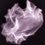
Crumpled graphene balls for high surface area applications
How often have you crumpled a sheet of paper in frustration and thrown it into the bin without further thought? You'll be amazed to hear that researchers - inspired by a trash can full of crumpled-up papers - have now applied this to solving one of the challenges of scaling up production of graphene sheets. One of the fascinating properties of crumpled paper balls is their strain-hardening effect - the harder you compress them, the stiffer they become, due to the formation of folded ridges that increase the strength. A similar effect has now been found in crumpled graphene balls. These crumpled particles exhibits strain-hardening behaviors, thus making them remarkable resistant to aggregation in both solution and dried states.
October 18, 2011
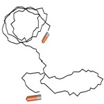
Autonomous nanomotor based on a true nanobattery
The catalytic conversion of chemical to mechanical energy, which is ubiquitous in biological systems, also is the basis for many of the engine systems that nanotechnology researchers are developing. Catalytic 'engines' will be key components of active micron- and sub-micron scale systems for controlled movement, particle assembly, and separations. So far, most of these catalytic micro- and nanomotors use hydrogen peroxide as the fuel. The major problem associated with this is that the produced oxygen bubbles make the observation and detailed study of these motors difficult. Researchers at the Pennsylvania State University have now introduced a new bubble-free, high efficient nanomotor system that involves the operation of a miniaturized copper-platinum nanobattery.
October 17, 2011
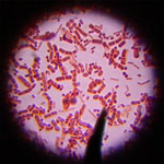
Nanomaterials help in early diagnosis of Meningitis
In order to enhance the utilization of nanomaterial in biological systems, it is very important to understand the influence they impart on cellular health and function. Nanomaterials present a research challenge as very little is known about how they behave in relation to micro-organisms, particularly at the cellular and molecular levels. Most of the nanomaterials reported earlier have demonstrated to be efficient antimicrobial agents against virus, bacteria or fungus. There are scarce research reports on the growth-promoting role of nanomaterials especially with respect to microbes. Recent findings, however, have challenged this concept of antimicrobial activity of nanoparticles.
October 13, 2011

Biofunctionalized silk nanofibers to repair the optic nerve
A main difference between central and peripheral nervous system is the lack of regeneration after a neurotrauma, leading to severe and irreversible handicaps. While biomaterials have been developed to aid the regeneration of peripheral nerves, the repair of central nerves such as the optic nerval or nerve cells in the spinal cord remain a major challenge for scientists. The ability to regenerate central nerve cells in the body could reduce the effects of trauma and disease in a dramatic way and nanotechnologies offer promising routes for repair techniques. Scientists have now attempted to rescue retinal ganglion cell death and enhance their regeneration using an electrospun material made of biofunctional nanofibers.
October 12, 2011
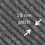
Lithography using neon ions achieves efficient exposure and high resolution
Cost of ownership has become a critical challenge facing future research in nanofabrication. As potential applications have broadened beyond the high-volume manufacture of integrated circuits, demand has increased for a robust tool capable of lithography at high pattern density and fidelity but also at low cost and thus suitable for scientific research, rapid prototyping, and low-volume manufacturing. Unfortunately, current manufacturing technologies employed in the chip industry are anything but 'low cost'. Researchers have now demonstrated a new source for lithography that has both higher per-particle exposure efficiency and a higher brightness than the sources conventionally used for lithography at the 10 nm scale.
October 11, 2011