Nanotechnology Spotlight – Latest Articles
 Subscribe to our Nanotechnology Spotlight feed
Showing Spotlights 2473 - 2480 of 3575 in category All (newest first):

Rapid probing of single molecules with a nanomechanical interface
The complex processes inside living systems emerge from the interactions of countless molecules. Understanding these interactions at the single molecule level is of great importance because mechanisms governing their function can be revealed best by interrogating individual molecules. Scientists rely on single-molecule techniques that allow them to isolate individual molecules and sequentially transport them for measurement and, potentially, manipulation. Most commonly, molecules are interfaced with tools like optical tweezers and atomic force microscopes. These devices are precision force sensors. Many interactions among biological molecules are short lived. Their lifetimes can be as short as a nanosecond. The existing single molecule techniques are limited in their temporal resolution, probing the timescales on the order of several milliseconds to a second. In new work, researchers have extended the reach of single molecule experiments to the microsecond timescale.
March 28, 2011
Graphene mass production comes closer with bulk wet chemical exfoliation of graphite
There are already several technologies that potentially allow mass production of graphene sheets; several of them are processing graphene in solution by exfoliating graphite. The general problem with this approach is however that is has been so far impossible to regenerate the undisturbed graphene lattice which was present prior to oxidation as decarboxylation inevitable takes place in the reduction step. In new work, researchers have now demonstrated the first bulk wet chemical exfoliation of graphite in association with an in situ covalent functionalization of intermediately generated graphene. With this novel chemical method, it is now possible to achieve covalently bonded functionalities without mechanical or sonochemical treatment. The covalent functionalization also protects the single-layer graphene from reaggregation and substrate-induced doping.
March 25, 2011

Unzipping carbon nanotubes could lead to superior artificial muscle systems
In the decades-old quest to build artificial muscles, many materials have been investigated with regard to their suitability for actuator application (the ability of a material to reversibly change dimensions under the influence of various stimuli). Recently, hope in obtaining improved artificial muscles was revitalized by the discovery of the extraordinary mechanical and electrical properties of graphene and its chemical derivatives. A new study shows that electrical heating of graphene oxide nanoribbons mats results in reversible generation of 1.6% stress and maximum work capacity of about 40 J/kg, which is similar to that of natural muscle. Unlike previous studies, the team obtained the graphene material by chemical unzipping of multi-walled carbon nanotubes.
March 24, 2011
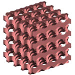
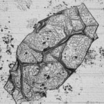
Novel 3D sculpturing of photonic crystals promises functionality at visible wavelengths
Photonic crystals are used to guide and localize light for all-optical processing of signals/information; to engineer dispersion and slow light; to harvest light (collect and redirect); and thresholdless lasing, that can be engineered by setting spectral ranges where light can be emitted. so far, there have been no demonstrations of full photonic bandgap at visible wavelengths - i.e., that at a certain visible range (between 400 nm to 780 nm) determined by the 3D photonic crystal structure, the light is rejected (reflected) at all angles of incidence. Researchers have now used a 3D nano-sculpturing process to fabricate 3D photonic crystal. The great potential of these 3D photonic crystal lies in the possibility to control light on a sub-wavelength scale.
March 23, 2011
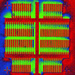
CMOS-compatible assembly of semiconducting single-walled carbon nanotube devices
The commercial realization of carbon nanotube-based electronic devices and their integration into the existing silicon-based processor technologies is still hampered by the inability to scale up the - currently lab-based - fabrication processes to manufacture a large number of devices on a single chip. The fundamental issue of carbon nanotube device fabrication still remains the biggest challenge for effective commercialization of nanotube electronics. In a further step towards large-scale integration of single-walled carbon nanotubes (SWCNTs) into complex functional electronic circuits, researchers have now combined a previously developed dielectrophoretic deposition approach with SWCNT sorting using density gradient ultracentrifugation, ensuring high purity of SWCNTs in suspension and consequently in the assembled devices.
March 22, 2011
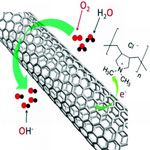
Role of intermolecular charge transfer promises efficient metal-free catalysts
The efficiency of catalyzing the oxygen reduction reaction (ORR) - the process that breaks the bonds of oxygen molecules - to a large degree determines the electrochemical performance of fuel cells. Platinum and platinum-based composites have long been considered as the most efficient ORR catalysts. In their search for practically viable non-precious metal ORR catalysts, researchers have also been investigating vertically-aligned nitrogen-containing carbon nanotubes. Having a strong electron-withdrawing ability, poly(diallyldimethylammonium chloride) (PDDA) was used to create net positive charge for carbon atoms in the nanotube carbon plane via intermolecular charge transfer. The resultant PDDA functionalized/adsorbed carbon nanotubes were demonstrated to act as metal-free catalysts for oxygen reduction reaction in fuel cells with similar performance as platinum catalysts.
March 21, 2011

Breakthrough makes large bandgap materials useful for photovoltaics
In a standard dye sensitized solar cell, an organic molecule adsorbed on the surface of a porous electrode absorbs light and then initiates the charge separation process eventually leading to generation of photocurrent. While the dye appears to have "sensitized" the large bandgap material, it never actually does, because only the dye molecules absorb the light and generate the carriers, the large bandgap material primarily serves the function of a conducting channel to take the electrons out. While wide bandgap materials alone can not absorb the sun light efficiently, it has been predicted that if two large bandgap materials with type-II band alignment form coaxial nanowires, the effective indirect bandgap could be substantially smaller than either of the individual materials. After a few years effort, one research team has now demonstrated a real functional device that exhibits the key feature of the idea: the use of two large bandgap materials to make a solar cell behaving like a small bandgap material.
March 18, 2011
A biophysical perspective of understanding nanoparticles at large
At the core of research efforts to determine the impact of synthetic nanoparticles on the environment and living systems is a fundamental understanding of the interactions between man-made nanoparticles and natural living systems that have evolved over millions of years. To describe nanoparticles at large, it may be beneficial to acknowledge that 1) biological systems are part of the food chain and therefore an essential component of the ecosystems and 2) collaborations are essential for such interdisciplinary research. Researchers have now presented a biophysical perspective that describes the fate of nanoparticles in both the aqueous phase and in living systems.
March 16, 2011