Showing Spotlights 49 - 56 of 161 in category All (newest first):
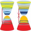
 Scientists have experimentally realized a plasmonic aerosol by efficiently transitioning liquid suspensions of gold nanorods into the gas phase and simultaneously measuring their optical spectra. They demonstrated that these aerosols are optically homogeneous, thermodynamically stable, with wide wavelength tunability (by controlling the aspect ratio of the nanorods) and have extremely large sensitivities to their environment. This novel plasmonic material could potentially open the door to many interesting applications ranging from geoengineering, vacuum microelectronics, molecular diagnostics, nanomedicines, nanojet printing and nonlinear optics.
Mar 6th, 2019
 Researchers demonstrate a display pixel that can switch on and off at least 1000 times faster than pixels that use conventional liquid crystal materials. They show that plasmonic gold nanorods - which interact very strongly with light - can be aligned using electric fields, and they use this alignment to control the amount of light that can pass through the pixel. By engineering the dimensions and material structure of the nanorods, the scientists design pixels that work with different colors of light, both visible and infrared.
Mar 4th, 2019
 Researchers report an interesting phenomenon of two-dimensional (2D) hexagonal boron nitride (h-BN)-induced planar-alignment of a nematic liquid crystal and the subsequent optical and electro-optical effects. Liquid crystals (LCs) are optically anisotropic materials, and they are widely used in electro-optical display technology, known as liquid crystal displays (LCDs). Understanding the alignment phenomena of a nematic LC on a surface remains an important area of research, as the alignment process determines the LC's molecular orientation and conformation - which influence the LC's optical and electro-optical characteristics in LCDs.
Jan 9th, 2019
 Motivated by the outstanding performance of graphene, graphene-like 2D materials have been intensively investigated, such as topological insulators, transition metal dichalcogenides (TMDs) and black phosphorous. Recently, 2D titanium disulfide, a typical TMD, is found to have strong light absorption properties from visible to infrared region, which is highly attractive for applications in nonlinear photonics. Researchers have fabricated a novel saturable absorber device is successfully fabricated based on 2D TiS2 nanosheets for ultrashort pulse generation and all-optical thresholding at the communication band.
Dec 27th, 2018
 Over the past several years, metal nanoparticles photosensitization over semiconductors with a large band gap has emerged as a promising strategy for developing visible-light responsive photocatalytic materials. In new work, researchers demonstrate a new plasmonic metamaterial can absorb nearly 100% of incident light (of a specific color) and use this energy to accelerate the production of chemicals. In constructing the near-perfect absorber, the researchers employ gold nanoparticles, TiO2 as the spacer layer, and a continuous gold thin film as the rear reflective layer.
Nov 28th, 2018
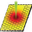
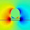 Researchers have developed a new type of optical manipulation method to achieve versatile manipulation of objects with different sizes and types using optical heating. In this new technique, nanoparticles get trapped at temperature hot spots instead of electrical hot spots, which demonstrates a different working mechanism and approach from the traditional optical manipulation techniques. Due to this unique working principle, stable trapping of large metallic nanoparticles and miniscule quantum dots on single nanoantennas with extremely low optical power is achieved.
Oct 3rd, 2018
 Recently developed concepts in photonic designs and meta- and nanomaterials have improved the effectiveness of passive radiative coolers that function in the daytime. Whereas all of these radiative coolers are white or silver in color, researchers have now presented concepts and strategies for daytime radiative cooling systems that offer aesthetically desirable colors and patterns. These device not only emit infrared waves effectively under a clear sky, but also displays vivid colors.
Sep 6th, 2018
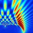
 Researchers have developed an all-optical lithographic technique called 'optothermoplasmonic nanolithography' (OTNL) to achieve high-throughput, versatile, and maskless patterning of different atomic layers. Taking graphene and molybdenum disulfide monolayers as examples, the team shows that both thermal oxidation and sublimation in the light-directed temperature field can lead to direct etching of the atomic layers. They further demonstrates programmable patterning of 2D materials into complex and large-scale nanostructures by steering the laser beam.
Aug 14th, 2018
 Subscribe to our Nanotechnology Spotlight feed