Deep Reactive Ion Etching (DRIE): Bosch Process, Cryogenic DRIE, and Applications
What is Deep Reactive Ion Etching?
Deep reactive ion etching (DRIE) is a highly anisotropic plasma etching process that creates deep, near-vertical features in silicon and related microfabrication materials.
DRIE extends ordinary reactive ion etching by adding a durable sidewall-protection mechanism. In a conventional RIE process, reactive radicals and directional ion bombardment remove material from exposed regions of a wafer, but the etch normally becomes difficult to keep vertical as the feature gets deeper. DRIE solves this by protecting the sidewalls while allowing the trench bottom to remain exposed to ion-assisted etching. The result is a process that can etch tens to hundreds of micrometers into silicon while preserving nearly vertical profiles.
In production, DRIE commonly reaches depths from several tens to several hundreds of micrometers. Specialized recipes can go deeper or reach much higher aspect ratios, but the result depends strongly on feature width, mask material, pattern density, wafer temperature, plasma source design, and how the recipe is tuned during the etch. This dependence is why DRIE is best understood not as one fixed recipe, but as a family of high-aspect-ratio plasma etching methods.
The two dominant routes for deep silicon plasma etching are the Bosch process and cryogenic DRIE. The Bosch process, patented by Franz Laermer and Andreas Schilp at Robert Bosch GmbH in 1996, alternates short etch and passivation steps. Cryogenic DRIE, developed in the same general period by academic and industrial plasma-etching groups, with important early work associated with the University of Twente, uses a continuous fluorine-and-oxygen plasma at very low wafer temperature. Bosch DRIE is especially common in production MEMS foundries, while cryogenic and related mixed-mode processes are often chosen when smoother, non-scalloped sidewalls are more important than maximum throughput. DRIE is now a central top-down manufacturing technique used in a cleanroom alongside photolithography, thin-film deposition, and wafer bonding.
Why it matters: DRIE made it possible to manufacture tall, narrow silicon structures with vertical walls. That capability underpins many MEMS sensors, through-silicon vias, silicon microfluidic devices, photonic structures, and silicon nanostructure arrays.
Key takeaways:
- DRIE is an anisotropic plasma process for deep, vertical-walled features, especially in silicon.
- The Bosch process alternates SF6 etching and C4F8 passivation, leaving characteristic sidewall scallops.
- Cryogenic DRIE uses a continuous SF6/O2 plasma at roughly −100 to −120 °C and can produce smoother, non-scalloped sidewalls.
- Pseudo-Bosch or mixed-mode DRIE balances etching and passivation at the same time, which can help with small features where Bosch scallops would be too large.
How the Bosch Process Works
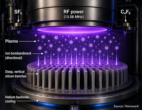
The Bosch process obtains its strong directionality by separating silicon removal and sidewall protection into alternating gas pulses, typically repeated hundreds or thousands of times. During the etch step, sulfur hexafluoride (SF6) is dissociated in an inductively coupled plasma into fluorine radicals and ions. Fluorine reacts with exposed silicon to form volatile silicon tetrafluoride (SiF4), which is removed by the vacuum system.
During the passivation step, octafluorocyclobutane (C4F8) deposits a Teflon-like fluorocarbon polymer on the mask, trench floor, and sidewalls. When the next SF6 etch step begins, ions accelerated toward the wafer clear the polymer preferentially from horizontal surfaces, especially the trench bottom. The sidewall coating remains largely intact, so the trench grows downward instead of widening sideways.
The unavoidable signature of this switched process is the sidewall scallop: a small periodic indentation that records each etch-passivation cycle. Reported scallop sizes often fall in the tens to hundreds of nanometers, with many MEMS processes producing scallops on the order of 50–200 nm. Shorter cycles reduce scallop size, but they also reduce average etch rate and can make the process more sensitive to timing, gas switching, and chamber conditions. For most MEMS devices the scallops are acceptable; for photonic, optical, fluidic, or precision-mechanical structures they may increase scattering, drag, surface area, or mechanical loss.
Bosch DRIE is popular because it is fast, robust, and mature. Industrial silicon Bosch recipes often etch at several to tens of micrometers per minute, and optimized processes can show high selectivity to hard masks such as silicon dioxide. Exact rates and selectivities should be treated as recipe-specific rather than universal: mask erosion, feature width, loading, platen power, pressure, and gas timing all change the outcome.
How Cryogenic DRIE Differs
Cryogenic DRIE replaces the switched Bosch sequence with a continuous plasma, usually based on SF6 and O2, while the wafer is clamped to a chuck cooled to roughly −100 to −120 °C. At these temperatures, oxygen and fluorine form a thin silicon oxyfluoride (SiOxFy) layer on the silicon surface. This passivation layer is stable on the cold sidewalls but is removed from the trench bottom by directional ion bombardment, allowing the etch front to continue downward.
Because there is no repeated etch-passivation cycle, cryogenic DRIE can produce smoother, non-scalloped sidewalls and avoids the fluorocarbon polymer residues associated with Bosch processing. That makes it attractive for optical and nanoscale structures where periodic sidewall roughness is undesirable. Optimized cryogenic recipes have also reported high mask selectivity, including roughly 100:1 selectivity to photoresist in some silicon processes and much higher values with metal hard masks. Such numbers are not general specifications; they depend on mask material, feature size, ion energy, wafer cooling, and chamber design.
The trade-off is a narrower process window. Wafer temperature, helium backside cooling, oxygen flow, and bias power must be tightly controlled. Too little passivation can produce undercut sidewalls, while too much passivation can lead to micromasking and "black silicon," a forest of needle-like silicon features caused by local etch inhibition. Even small thermal or gas-flow changes can move the process from vertical etching to taper, undercut, roughness, or grass formation.
What Is Pseudo-Bosch DRIE?
A third family of processes is often called pseudo-Bosch, mixed-mode DRIE, or continuous SF6/C4F8 etching. The terminology is not used uniformly across the literature. In this article, pseudo-Bosch refers to room-temperature, non-switched processes that feed etch and passivation gases at the same time, balancing silicon removal and polymer deposition continuously rather than in separate pulses.
Pseudo-Bosch can produce smoother, non-scalloped or only weakly textured sidewalls without cryogenic cooling. It is especially useful for small features where a 100 nm Bosch scallop would consume a large fraction of the linewidth. Its limitations are lower etch rates, a narrower tuning window, and more sensitivity to profile changes caused by loading and feature size.
Comparison of Bosch, Cryogenic, and Pseudo-Bosch DRIE
No single DRIE variant is best for every application. Throughput-driven MEMS production lines often use Bosch DRIE, while photonics, nanowire, and smooth-walled microfluidic processes may favor cryogenic or pseudo-Bosch approaches. The table below summarizes the main practical trade-offs.
| Process variant | Wafer temperature | Chemistry | Sidewall morphology | Strengths | Limitations |
|---|---|---|---|---|---|
| Standard Bosch | Usually near room temperature or moderately cooled | Alternating SF6 / C4F8 pulses | Periodic scallops, often tens to hundreds of nanometers | High throughput, mature tooling, strong verticality, robust for many MEMS processes | Scallops, fluorocarbon residues, RIE lag, possible notching at insulating layers |
| Cryogenic DRIE | Roughly −100 to −120 °C | Continuous SF6 / O2 | Smoother, non-scalloped, near-vertical when tuned well | Low polymer residue, high feature fidelity, useful for photonics and nanostructures | Requires cryogenic cooling, tight thermal control, risk of black silicon or undercut |
| Pseudo-Bosch / mixed mode | Usually room temperature | Simultaneous SF6 + C4F8 | Smoother than Bosch; may be slightly tapered | No cryostat, useful for sub-micrometer structures, reduced scalloping | Lower etch rate than Bosch and a narrower process window |
| Conventional RIE | Usually room temperature | Single-step fluorinated or chlorine-based plasma, depending on material | Often tapered or undercut for deep features | Simple, widely available, good for shallow pattern transfer | Not designed for sustained high-aspect-ratio sidewall protection |
The important trade-off is not simply "fast versus smooth." Bosch DRIE offers a wide, production-friendly process window but leaves a periodic sidewall texture. Cryogenic DRIE can improve sidewall smoothness and reduce polymer contamination, but it requires stricter thermal control. Pseudo-Bosch avoids switching and cryogenic operation, but it usually gives up some speed and can be less forgiving.
Key Process Parameters
Modern DRIE tools often use independent inductively coupled plasma (ICP) and radio-frequency bias generators. ICP power mainly controls plasma density and the supply of reactive species, while RF bias controls the ion energy striking the wafer. Higher plasma density can raise chemical etch rate; higher bias can improve bottom clearing and anisotropy, but it can also increase mask erosion, trench-bottom damage, microtrenching, and notching.
Chamber pressure controls the balance between gas transport, ion directionality, and scattering. Lower pressure generally improves ion directionality, which helps vertical profiles, while higher pressure can increase radical density and etch rate but may broaden ion trajectories. In deep trenches, both incoming reactants and outgoing by-products must travel through restricted openings, so transport limitations become more severe as aspect ratio increases.
Gas flow and timing set the etch-passivation balance. In Bosch DRIE, longer SF6 etch steps increase rate and scallop size, while longer C4F8 passivation steps push the profile toward more protected or even re-entrant sidewalls. In cryogenic DRIE, the SF6-to-O2 ratio plays an analogous role. Small oxygen-flow changes can move the profile from vertical to undercut or overpassivated.
Pattern density also matters. A wafer covered with open trenches consumes reactive species differently from a wafer with isolated openings, so etch rate can vary with layout. This loading effect is one reason DRIE recipes developed on test patterns may not transfer perfectly to product masks. Designers often add dummy features, adjust local pattern density, or use layout-specific process compensation to improve uniformity.
Wafer temperature ties the whole process together. In Bosch etching it affects polymer deposition and removal; in cryogenic DRIE it defines the very existence and stability of the passivation layer. Helium backside cooling is used to improve thermal contact between the wafer and chuck, because direct solid-solid contact is imperfect at the microscopic scale.
Materials Beyond Silicon
The term DRIE is most closely associated with high-aspect-ratio silicon etching. Related high-aspect-ratio plasma etching methods are also used for silicon dioxide, silicon nitride, silicon carbide, gallium nitride, polymers, and quartz, but these processes may not use the same Bosch or cryogenic mechanisms and often have lower etch rates or selectivities than silicon DRIE.
Silicon carbide etching for power electronics and harsh-environment MEMS typically requires higher ion energies because SiC is chemically and physically harder to etch than silicon. Quartz and other dielectric etches often use fluorocarbon chemistries with metal hard masks. Polymers may be etched with oxygen-containing plasmas, while compound semiconductors such as gallium nitride require chemistries tuned to their bond strengths and by-products. In each case, the core challenge is the same: remove material vertically from the trench bottom while preventing lateral erosion of the sidewalls.
Applications
MEMS sensors and actuators
DRIE is a foundational fabrication step for many silicon MEMS devices, including accelerometers, gyroscopes, microphones, pressure sensors, micromirrors, and resonators. The ability to form deep vertical trenches in single-crystal silicon allows engineers to define proof masses, springs, comb drives, membranes, and release structures with precise mechanical dimensions. Many MEMS devices are also integrated with CMOS readout electronics, making DRIE an important bridge between micromechanical structures and semiconductor manufacturing.
Through-silicon vias and 3D integration
Through-silicon vias (TSVs) are vertical electrical connections through a silicon wafer or die. They support 3D stacking of integrated circuits, image sensors, MEMS packages, and high-bandwidth memory. Bosch DRIE is commonly used to etch the via openings, which may range from a few micrometers to tens of micrometers in diameter and from tens to hundreds of micrometers deep. After etching, the vias are insulated, lined with barrier and seed layers by deposition methods such as CVD, PVD, or atomic layer deposition, and then filled, often by copper electroplating.
Microfluidics and biomedical devices
DRIE forms deep, straight-walled channels, chambers, nozzles, filters, and through-wafer ports in silicon-based lab-on-a-chip devices. Silicon is less flexible than polymer materials such as PDMS, but it offers dimensional precision, thermal stability, compatibility with wafer-scale processing, and integration with sensors or electrodes. DRIE is also used to fabricate hollow microneedle arrays, microfluidic interconnects, and biomedical membranes where high-aspect-ratio openings are needed.
Photonics, metasurfaces, and nanostructure arrays
Cryogenic and pseudo-Bosch processes are useful for photonic crystals, sub-wavelength gratings, waveguide structures, and silicon metasurfaces because sidewall roughness can scatter light and reduce device performance. The same high-aspect-ratio etching concepts are used to make dense silicon nanopillars and nanowire arrays for anti-reflection surfaces, battery electrodes, biosensors, and cell-culture scaffolds. These processes are often combined with nanopatterning methods such as electron-beam lithography or nanoimprint lithography. Nanopores and NEMS resonators can also use DRIE-derived processes when vertical nanoscale features are required.
Challenges and Limitations
The most common DRIE limitation is RIE lag, also called aspect-ratio-dependent etching. Narrow trenches often etch more slowly than wide trenches because neutral radicals, ions, and reaction products have more difficulty moving through high-aspect-ratio openings. The effect can create different final depths on the same wafer. Reported Bosch processes can show depth differences greater than 10 percent between features of different aspect ratios, while optimized ramped or multi-step recipes have reduced this lag to much lower levels in specific demonstrations.
A second limitation is notching, especially in silicon-on-insulator (SOI) wafers. When the etch front reaches the buried oxide, charge can accumulate on the insulating surface and deflect incoming ions sideways. This produces a lateral "foot" near the base of the trench, which can weaken released MEMS structures or change their dimensions. Bias pulsing, endpoint control, modified passivation, and layout changes are common mitigation strategies.
A third limitation is mask erosion. As features become deeper, the mask must survive longer exposure to ions, radicals, and polymer deposition/removal cycles. Photoresist may be adequate for many moderate-depth etches, but deeper or higher-selectivity processes often require silicon dioxide, silicon nitride, metals, or multilayer hard masks. At extreme depths, mask survival can set the practical limit before plasma transport does.
Other concerns include sidewall roughness, microtrenching at the trench bottom, polymer residue, wafer heating, chamber seasoning, across-wafer nonuniformity, and recipe drift during long campaigns. Extending DRIE-like methods to non-silicon materials, combining DRIE with atomic layer etching, and integrating DRIE with wet etching or focused ion beam milling remain active areas of process development.
FAQ: Deep Reactive Ion Etching
What is the difference between RIE and DRIE?
Reactive ion etching (RIE) is a plasma process that combines chemical etching by reactive species with directional ion bombardment. It is widely used for shallow or moderate-depth pattern transfer. Deep reactive ion etching (DRIE) adds sustained sidewall protection, either by alternating etch and passivation steps or by using temperature-dependent passivation, so that much deeper features can be etched while remaining nearly vertical.
Why does the Bosch process produce scallops on sidewalls?
The Bosch process alternates between an SF6 etch step and a C4F8 passivation step. Each cycle removes a small amount of silicon before the next polymer layer is deposited. The sidewall therefore records the repeated sequence as a small ripple or scallop. Shorter cycles can reduce scallop size, but they usually reduce etch rate and make the process more sensitive to timing.
How deep can DRIE etch into silicon?
Common production DRIE processes etch silicon from tens to several hundreds of micrometers deep. Specialized recipes can produce deeper through-wafer trenches or very high-aspect-ratio sub-micrometer features, including reported aspect ratios above 100 in optimized demonstrations. The practical limit depends on mask selectivity, feature width, aspect-ratio-dependent etching, wafer cooling, and reactor design.
What materials besides silicon can be etched with DRIE?
DRIE is most closely associated with silicon. Related high-aspect-ratio plasma etching methods are also used for silicon dioxide, silicon nitride, silicon carbide, gallium nitride, quartz, and polymers, but these materials need different chemistries and often different masks. Their etch rates and selectivities are usually lower or more process-specific than those of silicon.
What is RIE lag and why does it matter?
RIE lag is the tendency for narrow, high-aspect-ratio features to etch more slowly than wider openings on the same wafer. It happens because gases, ions, and by-products have more restricted transport in deep narrow trenches. RIE lag matters because it can leave different structures at different depths even when they were patterned and etched at the same time.
Why is helium used on the back side of the wafer during DRIE?
Helium backside cooling improves thermal contact between the wafer and the cooled electrostatic or mechanical chuck. Plasma etching deposits heat into the wafer, and wafer temperature strongly affects passivation, profile shape, and etch rate. Helium fills microscopic gaps between the wafer and chuck, helping the wafer stay close to the intended process temperature. This is especially important in cryogenic DRIE.
Further Reading
Journal of Applied Physics, High aspect ratio silicon etch: A review
Journal of Micromechanics and Microengineering, Black silicon method X: a review on high speed and selective plasma etching of silicon with profile control
Plasma Processes and Polymers, MEMS at Bosch – Si plasma etch success story, history, applications, and products
Applied Physics Reviews, Deep-reactive ion etching of silicon nanowire arrays at cryogenic temperatures
