Nanoimaging: Unveiling the Nanoscale World
What is Nanoimaging?
Nanoimaging refers to a collection of techniques and technologies used to visualize, characterize, and analyze structures and phenomena at the nanoscale. It encompasses various imaging methods that provide high-resolution images and information about the properties, behavior, and interactions of materials and systems at the nanometer level.
Importance of Nanoimaging
Nanoimaging plays a crucial role in the field of nanotechnology by enabling researchers to:
- Visualize Nanoscale Structures: Nanoimaging techniques allow researchers to directly observe and study the morphology, structure, and organization of nanomaterials, nanodevices, and biological systems at the nanoscale.
- Characterize Nanoscale Properties: Nanoimaging methods can provide quantitative information about various nanoscale properties, such as surface topography, chemical composition, electronic structure, and mechanical properties.
- Understand Nanoscale Interactions: Nanoimaging enables the investigation of interactions between nanoscale components, such as nanoparticles, biomolecules, and surfaces, providing insights into fundamental processes and mechanisms at the nanoscale.
- Guide Nanofabrication: Nanoimaging techniques are essential for guiding the fabrication and assembly of nanoscale structures and devices, allowing researchers to monitor and optimize the manufacturing processes.
Nanoimaging Techniques
Nanoimaging encompasses a wide range of techniques, each with its own strengths and limitations. Some of the most commonly used nanoimaging techniques include:
Electron Microscopy
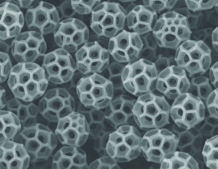
Electron microscopy techniques, such as scanning electron microscopy (SEM) and transmission electron microscopy (TEM), use focused electron beams to image nanoscale structures. SEM provides high-resolution surface imaging, while TEM enables the visualization of internal structures and atomic-scale features.
Scanning Probe Microscopy
Scanning probe microscopy techniques, including atomic force microscopy (AFM) and scanning tunneling microscopy (STM), use sharp probes to scan the surface of a sample and measure various properties. AFM can map surface topography and measure mechanical properties, while STM can image individual atoms and electronic states.
Optical Nanoscopy
Optical nanoscopy techniques, such as super-resolution microscopy and near-field scanning optical microscopy (NSOM), overcome the diffraction limit of light to achieve nanoscale resolution. These techniques enable the visualization of biological structures, such as proteins and DNA, with high specificity and contrast.
X-ray Imaging
X-ray imaging techniques, including X-ray diffraction (XRD), X-ray scattering, and X-ray tomography, use high-energy X-rays to probe the internal structure and composition of nanomaterials. These methods can provide information about crystal structure, phase composition, and 3D morphology.
Challenges and Future Directions
Despite the remarkable capabilities of nanoimaging techniques, several challenges remain. One of the main challenges is the trade-off between resolution and sample compatibility. High-resolution techniques often require specific sample preparation and imaging conditions that may not be suitable for all types of samples, particularly biological specimens.
Another challenge is the interpretation and analysis of nanoimaging data. The vast amount of information generated by nanoimaging experiments requires advanced computational tools and algorithms to extract meaningful insights and correlate the data with other characterization techniques.
Future developments in nanoimaging will focus on improving resolution, sensitivity, and speed while minimizing sample damage. The integration of multiple imaging modalities and the development of correlative nanoimaging approaches will provide a more comprehensive understanding of nanoscale systems. Additionally, the advancement of in situ and operando nanoimaging techniques will enable real-time observation of dynamic processes and reactions at the nanoscale.
Applications of Nanoimaging
Nanoimaging finds applications in various fields, including:
- Materials Science: Nanoimaging is essential for characterizing the structure, composition, and properties of nanomaterials, such as nanoparticles, nanowires, and thin films, guiding the development of advanced functional materials.
- Nanoelectronics: Nanoimaging techniques are used to visualize and analyze nanoelectronic devices, such as transistors and memory cells, enabling the optimization of device performance and reliability.
- Life Sciences: Nanoimaging plays a crucial role in studying biological systems at the nanoscale, including proteins, DNA, and cellular structures, contributing to advancements in molecular biology, drug discovery, and nanomedicine.
- Energy and Environment: Nanoimaging is applied to investigate nanoscale phenomena in energy conversion and storage devices, such as solar cells and batteries, as well as to study the environmental impact and fate of nanomaterials.
