Nanomembranes: Definition, Fabrication, Properties, and Applications
What is a Nanomembrane?
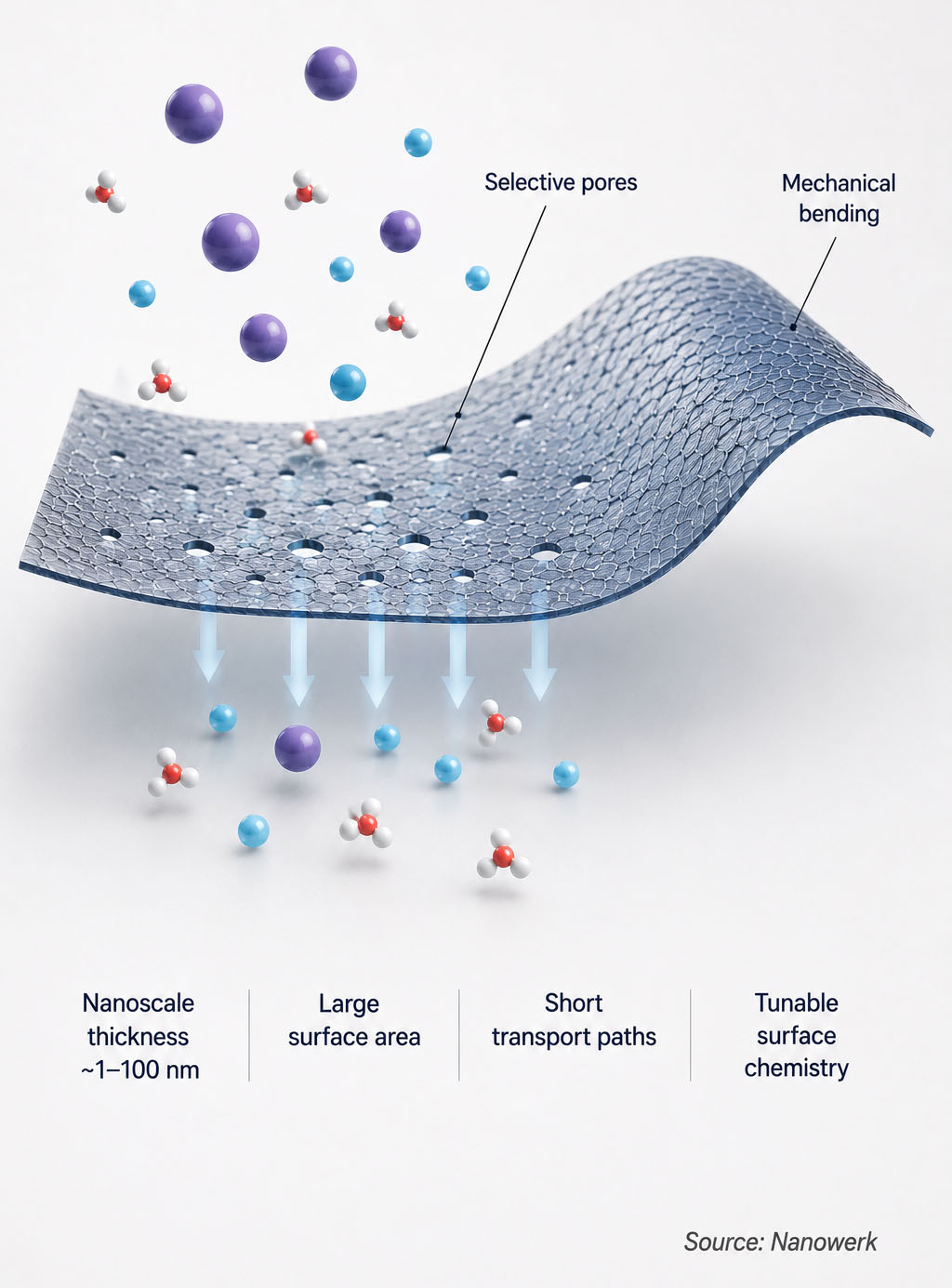
In one sentence: A nanomembrane is an ultrathin sheet with nanoscale thickness and much larger lateral dimensions, used as a selective separation barrier, a flexible substrate for electronics and sensors, or an active device layer that exploits short transport distances and large surface area.
A nanomembrane is an ultrathin, sheet-like material whose thickness is in the nanoscale while its length and width are much larger.
In strict nanotechnology terminology, the closest shape class is a nanoplate-like nano-object: one external dimension is nanoscale and the other two are significantly larger. Nanomembrane is the application-oriented term used when such an ultrathin sheet acts as a selective barrier, flexible substrate, biointerface, support layer, transferable device layer, or active sensing surface. It is therefore helpful to distinguish three overlapping ideas: a nanoplate-like nano-object is a formal shape category, a thin film is often a substrate-bound coating or device layer, and a nanomembrane is an ultrathin sheet whose membrane-like function is central.
There is no single universal thickness cutoff. Strictly, nanoscale thickness usually means roughly 1–100 nm. In practice, many communities also call freestanding, transferable, or mechanically compliant sheets several hundred nanometers thick nanomembranes when their transport, mechanics, or electronic behavior is governed by ultrathin geometry. Lateral sizes can range from micrometers to full silicon wafers.
Nanomembranes span a remarkable breadth of chemistry. Polyamide layers a few tens of nanometers thick form the active barrier in commercial reverse osmosis modules, single-crystal silicon sheets released from silicon-on-insulator wafers carry flexible transistors, and two-dimensional materials such as graphene, hexagonal boron nitride, and transition metal dichalcogenides become nanomembranes when they span an opening, act as a barrier, or are assembled into transferable sheets.
Key takeaways:
- Nanomembranes are sheets with nanoscale thickness, used as freestanding or loosely supported layers rather than as substrate-bound coatings.
- Their nanoscale thickness gives short transport paths, mechanical flexibility, strain tunability, and direct coupling to the environment on both faces.
- Fabrication routes include thinning of bulk films, atomic-scale deposition, layer-by-layer assembly, interfacial polymerization, and assembly of exfoliated 2D nanosheets.
- Applications include water and gas separation, flexible and biointegrated electronics, biomedical scaffolds and wound dressings, sensors, and energy devices.
| Feature | Typical meaning |
|---|---|
| Thickness | Roughly 1–100 nm in strict nanoscale usage; sometimes several hundred nanometers in device and membrane literature when ultrathin geometry controls behavior |
| Lateral size | Micrometers to wafer scale or module scale |
| Key distinction | Sheet functionality: selective barrier, released film, flexible substrate, biointerface, or active device layer rather than merely a substrate-bound coating |
| Main uses | Water and gas separation, sensing, flexible electronics, biointegrated devices, wound care, and energy systems |
Why Thinness Matters at the Nanoscale
Reducing the thickness of a sheet from micrometers to nanometers changes several properties at once. All else being equal, diffusive resistance scales roughly with thickness, so a 50 nm dense polymer layer can in principle provide far higher permeance than a 5 µm film of the same chemistry. In real membranes, support resistance, defects, swelling, concentration polarization, fouling, and interfacial resistance often limit how much of this theoretical gain is realized. Surface-to-volume ratio rises sharply, so two parallel interfaces dominate the response of the sheet and interface chemistry can be tuned to control permeability, fouling resistance, and biocompatibility.
Mechanical behavior also changes. A continuous sheet that is a few hundred nanometers thick can be bent to radii below a millimeter without exceeding the fracture strain of even brittle inorganic semiconductors, because the strain at the outer surface of a bent sheet scales with thickness divided by bending radius. This is the geometric basis for flexible single-crystal silicon and gallium arsenide electronics. The same geometry makes nanomembranes responsive to strain engineering: lattice mismatch between stacked layers, or controlled buckling on a soft substrate, applies large reversible strains that shift band gaps, magnetic order, or piezoelectric response.
Sub-100 nm thickness also brings membranes into regimes where confinement effects matter. Ångström-scale slit channels between stacked 2D nanosheets and the dense aromatic networks of polyamide reverse-osmosis skins can transport water, ions, and gases through pathways comparable to molecular dimensions or hydration-shell dimensions, so classical solution-diffusion descriptions may be complemented by size-dependent and chemistry-dependent sieving. Quantum confinement in single-crystalline semiconductor nanomembranes thinner than the exciton Bohr radius can shift band gaps and absorption spectra in ways not possible in bulk wafers.
Common Nanomembrane Material Classes
Nanomembranes are made from almost every class of solid material, with the choice dictated by the application: polymers for separations and biomedical uses, 2D materials for high-flux selective membranes, inorganic semiconductors for flexible electronics, and metal-organic and covalent-organic frameworks for chemically programmable porosity.
| Material class | Typical thickness | Main fabrication route | Key properties | Representative uses |
|---|---|---|---|---|
| Polyamide active layers and polymer membrane systems (PA, PVDF, PSf, PEI, polyimide) | 20–200 nm selective skin or active layer on micrometer-scale porous support | Interfacial polymerization, phase inversion | High selectivity when used as dense active skins; mature supports and module manufacturing | Reverse osmosis, nanofiltration, ultrafiltration, gas separation |
| Block copolymer membranes (PS-b-PMMA, PS-b-P4VP, PI-b-PS-b-PEO) | 30–500 nm | Self-assembly, selective swelling or etching, block-copolymer lithography | Narrow pore-size distribution, tunable chemistry, vertical channels | Ultrafiltration, virus removal, drug-release devices |
| 2D material laminates (graphene oxide, MXene, h-BN, MoS2, COF nanosheets) | 1–100 nm | Liquid-phase exfoliation, vacuum filtration, layer-by-layer assembly | Ångström-scale interlayer channels, tunable surface chemistry, ion sieving | Desalination, organic-solvent nanofiltration, gas separation |
| Single-crystal semiconductor nanomembranes (Si, Ge, GaAs, GaN, InP) | 10–500 nm | Release from silicon-on-insulator or epitaxial sacrificial layers, transfer printing | Bulk-like carrier mobility, mechanical flexibility, strain tunability | Flexible transistors, photodetectors, biointegrated electronics |
| Ceramic and oxide nanomembranes (SiO2, Al2O3, TiO2, ZrO2, zeolite) | 5–200 nm | Atomic layer deposition, sol-gel, hydrothermal growth | Thermal and chemical stability, well-defined pores, photocatalytic activity | Gas separation, harsh-environment filtration, catalytic membranes |
| Framework membranes (MOF, COF, zeolite) | 10–200 nm | In-situ growth on porous support, exfoliated nanosheet assembly | Crystallographically defined pores, chemical tunability | Gas separation, hydrogen purification, organic-solvent nanofiltration |
| Bioresorbable polymer membranes (PCL, PLA, PLGA, silk fibroin, chitosan) | 50–500 nm | Spin coating, dip coating, electrospinning of thin layers | Biocompatibility, controlled degradation, drug loading | Wound dressings, transient implants, tissue interfaces |
Most practical nanomembranes are not single-component. A reverse osmosis module combines a nanometer-thick aromatic polyamide active layer with a microporous polysulfone support and a polyester backing; PVDF, PSf, PEI, and related polymers often act as porous supports or ultrafiltration membranes rather than as the nanometer-scale selective skin itself. A flexible silicon nanomembrane device adds dielectric, contact, and encapsulation layers around the active sheet.
How Nanomembranes Are Made
Fabrication routes fall into four broad families, and the right choice depends on the material, the thickness required, and whether the membrane will be used as a coating, a freestanding sheet, or an embedded device layer.
Top-down thinning and release
For single-crystal semiconductors, the most common starting point is a silicon-on-insulator wafer or an epitaxial multilayer with a buried sacrificial layer. Selective wet or vapor etching of the buried oxide or release layer frees the top crystalline layer as a sheet that can be transferred to a target substrate using elastomeric stamps. This approach gives access to nanomembranes of silicon, germanium, gallium arsenide, gallium nitride, and indium phosphide with bulk-like crystal quality and thicknesses set by the original epilayer.
Atomic-scale and vapor-phase deposition
Atomic layer deposition (ALD) builds inorganic nanomembranes from sequential, self-limiting surface reactions, giving conformal coverage and Ångström-level thickness control. ALD on a sacrificial template followed by template removal yields freestanding oxide nanomembranes. Chemical vapor deposition is the workhorse for monolayer and few-layer 2D materials such as graphene and the transition-metal dichalcogenides; growth on a metal catalyst followed by polymer-assisted transfer produces large-area atomically thin nanomembranes.
Solution and interfacial chemistry
Many polymer nanomembranes are produced by interfacial polymerization, in which two reactive monomers dissolved in immiscible solvents meet at the liquid-liquid interface and form a dense crosslinked film a few tens of nanometers thick. This is the foundation of the polyamide active layer in commercial reverse osmosis. Layer-by-layer assembly builds membranes one polyelectrolyte or nanosheet at a time from aqueous solution, with thickness controlled to within a few Ångströms. Block-copolymer self-assembly generates regular arrays of cylindrical or lamellar microdomains; selective removal of the minority block leaves a nanoporous membrane with pore diameters typically between 5 and 50 nm.
2D nanosheet assembly
For laminar 2D membranes, the active material is first produced as a dispersion of nanosheets by liquid-phase exfoliation of layered crystals such as graphite, hexagonal boron nitride, transition-metal dichalcogenides, MAX phases (for MXenes), or layered MOFs and COFs. The dispersion is then deposited on a porous support by vacuum filtration, blade casting, spray coating, or spin coating to give a stacked laminate with restored interlayer spacing. Pore engineering by chemical functionalization, ion intercalation, or controlled defect creation tunes the slit channels between the sheets to match the size and charge of the target permeant.
Applications
Water and ion separation
Membrane-based water treatment is by far the largest application of nanomembranes. Polyamide thin-film composite membranes with active layers a few tens of nanometers thick provide the dense barrier in reverse osmosis modules used for seawater desalination, brackish-water purification, and industrial water reuse, and similar architectures with looser chemistries are used for nanofiltration and ultrafiltration. Research nanomembranes built from graphene oxide laminates, MXene films, COF and MOF nanosheets, and aquaporin-decorated layers have shown selective rejection of ions, organic micropollutants, and oil emulsions in laboratory tests, with the central challenge being to translate these results into scalable, fouling-resistant, defect-free modules.
Gas separation and energy carriers
Nanomembranes built from glassy polymers, polymers of intrinsic microporosity, MOF and zeolite layers, and stacked 2D nanosheets are used to separate gas mixtures such as carbon dioxide from nitrogen, oxygen from nitrogen, and hydrogen from larger gases. Reducing the membrane thickness while preserving intrinsic selectivity can raise permeance and help materials approach or exceed practical selectivity-permeability trade-offs, lowering the energy cost of capture, purification, and natural-gas upgrading. The same architectures are being explored for helium recovery and upgrading green hydrogen from electrolysis.
Flexible and biointegrated electronics
Silicon and compound-semiconductor nanomembranes released from rigid wafers and transferred to plastic, rubber, or biodegradable substrates carry transistors, diodes, photodetectors, and solar cells that bend, fold, and stretch while keeping bulk-like electrical performance. This is the technological basis for skin-mounted health sensors, conformal cardiac and neural arrays, and curvilinear photodetector cameras, complementing other flexible and stretchable electronics approaches that use small-molecule, polymer, or printed inorganic materials.
Biomedical membranes and drug delivery
Bioresorbable polymer nanomembranes made from polycaprolactone, polylactic acid, polylactic-co-glycolic acid, and silk fibroin act as tissue interfaces, conformal wound dressings, and barrier layers in guided tissue regeneration. Their submicron thickness lets them adhere to skin and internal tissues without mechanical mismatch, while their large two-faced surface area can be loaded with antibiotics, growth factors, or small-molecule drugs for sustained release in targeted delivery. Polymer nanomembranes also serve as protective and dialysis-like layers around cell encapsulation devices and implantable sensors that need molecular access without immune attack.
Sensors, actuators, and energy storage
The two accessible faces of a nanomembrane make it a natural transducer between an external environment and an electrical readout. Field-effect biosensors built on silicon nanomembranes detect biomolecules at very low concentrations because the depletion region spans the entire sheet, and flexible piezoelectric and triboelectric nanomembranes act as nanogenerators harvesting energy from motion. In batteries, supercapacitors, and fuel cells, nanomembrane separators and electrolyte layers reduce internal resistance and improve safety.
Challenges and Future Perspectives
Several issues continue to shape the field. Scaling defect-free 2D-material nanomembranes from centimeter-scale laboratory coupons to the square-meter modules required by water and gas industries remains difficult, because a single tear or pinhole can dominate selectivity over an entire device. Long-term chemical and mechanical stability under realistic conditions, in particular oxidation of MXenes and swelling of graphene oxide laminates, has driven a wave of crosslinking and hybridization strategies.
Transfer and handling of freestanding sheets are routinely the rate-limiting step for semiconductor nanomembrane electronics, with deterministic pick-and-place transfer, roll-to-roll lamination, and direct epitaxial release on flexible carriers all under active development. In 2D membranes, defect engineering has shifted from a problem to a design parameter, where controlled vacancies and functional groups define the slit channels, although reproducibility across batches still constrains industrial uptake.
The field is moving toward multifunctional, heterogeneously stacked architectures rather than single-component sheets. Mixed-matrix designs combine the processability of polymers with the selectivity of MOF or 2D fillers; biointegrated stacks combine silicon nanomembrane logic, bioresorbable encapsulation, and antifouling polymer top layers in one conformal device; and machine-learning-assisted screening of polymer chemistries and 2D building blocks is shortening the cycle between target performance and a candidate membrane.
FAQ: Nanomembranes
What is the difference between a nanomembrane and a thin film?
Both have nanoscale thickness, but the terms emphasize different things. A thin film is generally a coating bonded to a substrate and judged by its surface and interface properties, while a nanomembrane is designed to function as a sheet with two accessible faces and is usually transferred or released from its growth substrate to act as a freestanding or supported sheet. In practice, the categories overlap, and the same material can be called a thin film during deposition and a nanomembrane after release.
How thick is a nanomembrane?
There is no single universal cutoff. Strict nanotechnology usage usually treats the nanoscale as roughly 1–100 nm, but many research communities also describe freestanding, transferable, or device-active sheets several hundred nanometers thick as nanomembranes when their behavior is governed by ultrathin geometry. Lateral dimensions can extend from micrometers to wafer scale.
Can nanomembranes desalinate seawater?
In principle, and in many laboratory demonstrations, yes. Graphene oxide laminates, MXene films, and tailored polymer nanomembranes have shown ion rejection from saline solutions. However, large-scale seawater desalination is still dominated by polyamide thin-film composite reverse-osmosis membranes. Research nanomembranes must still prove defect-free scale-up, chemical stability, fouling resistance, pressure tolerance, and long operating lifetimes.
Are nanomembranes used in commercial products?
Yes, but the wording needs care. Polyamide active layers in reverse-osmosis and nanofiltration modules are established commercial examples of nanometer-thick selective membranes. Some filtration products use nanoscale or nanostructured active layers, although many high-efficiency filters are better described as nonwoven fiber media rather than true nanomembranes. Silicon nanomembranes appear in flexible sensors and prototype implantable devices, and ultrathin polymer films are used in skin patches and wound-care products.
Why are 2D materials so attractive for nanomembranes?
Two-dimensional materials such as graphene, hexagonal boron nitride, transition metal dichalcogenides, MXenes, and 2D covalent organic frameworks are atomically thin sheets that become nanomembranes when they span an opening, act as a barrier, or are assembled into a transferable laminate. Their Ångström-scale interlayer channels and engineerable pores can give very high permeance and size- or charge-based selectivity. Practical use still depends on controlling defects, swelling, oxidation, mechanical damage, and scalable manufacturing.
Further Reading
Environmental Science: Water Research & Technology, Membrane materials for water purification: design, development, and application
Journal of the American Chemical Society, Semiconductor Nanomembrane Materials for High-Performance Soft Electronic Devices
Chemical Reviews, From Layered Crystals to Permselective Membranes: History, Fundamentals, and Opportunities
Advanced Functional Materials, Recent Progress on Flexible Silicon Nanomembranes for Advanced Electronics and Optoelectronics
