| Posted: May 05, 2015 |
Channeling valleytronics in graphene
|
|
(Nanowerk News) To the list of potential applications of graphene – a two-dimensional semiconductor of pure carbon that is stronger and much faster than silicon – we can now add valleytronics, the coding of data in the wavelike motion of electrons as they speed through a conductor. Berkeley Lab researchers have discovered topologically protected one-dimensional electron conducting channels at the domain walls of bilayer graphene. These conducting channels are “valley polarized,” which means they can serve as filters for electron valley polarization in future devices such as quantum computers.
|
|
“Combining near-field infrared nanometer-scale microscopy and low-temperature electrical transport measurements, we have recorded the first experimental observations of 1D ballistic electron conducting channels at bilayer graphene domain walls,” says Feng Wang, a condensed matter physicist with Berkeley Lab’s Materials Sciences Division, who led this work. “These 1D valley-polarized conducting channels featured a ballistic length of about 400 nanometers at 4 kelvin. Their existence opens up opportunities for exploring unique topological phases and valley physics in graphene.”
|
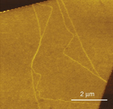 |
| In this near-field infrared nanoscopy image of bilayer graphene obtained at the Advanced Light Source, domain walls are revealed by bright lines that arise because of the walls’ electronic structures and IR responses.
|
|
Wang, who also holds an appointment with the University of California (UC) Berkeley Physics Department, is the corresponding author of a paper describing this research in the journal Nature ("Topological valley transport at bilayer graphene domain walls").
|
|
Valleytronics is generating a lot of excitement in the high-tech industry as a potential avenue to quantum computing. Like spintronics, valleytronics offers a tremendous advantage in data processing speeds over the electrical charge used in classical electronics.
|
|
“In valleytronics, electrons move through the lattice of a 2D semiconductor as a wave with two energy valleys, each valley being characterized by a distinct momentum and quantum valley number,” Wang says. “This quantum valley number can be used to encode information when the electrons are in a minimum energy valley.”
|
|
Recent theoretical work suggested that domain walls between AB- and BA-stacked bilayer graphene could provide an attractive place to realize one-dimensional electron conducting channels for valleytronics because the smoothness of the domain walls preserves electron valleys, unlike the atomic defects at graphene edges that result in valley-mixing. Until now, however, there has been no experimental evidence of these channels.
|
|
Working at Berkeley Lab’s Advanced Light Source (ALS), a DOE Office of Science User Facility, Wang, Ju, Shi and their colleagues used tightly focused beams of infrared light to image in situ bilayer graphene layer-stacking domain walls on device substrates. Field effect devices fabricated over these domain walls revealed the 1D conducting channels.
|
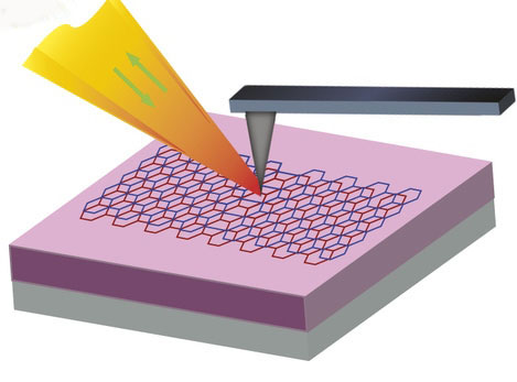 |
| In the bilayer graphene imaging work by Feng Wang and his group, IR light (yellow) is focused onto the apex of a metal-coated AFM tip and the backscattered infrared radiation is collected and measured.
|
|
“The infrared measurements were carried out at ALS beamline 5.4,” says Shi. “The near-field infrared capabilities of this beamline enable optical spectroscopy with spatial resolutions that are way beyond the diffraction limit, allowing us to image the nanometer-wide domain walls in bilayer graphene.”
|
|
To date, most valleytronics research has focused on the 2D semiconductors known as MX2 materials, which consist of a single layer of transition metal atoms, such as molybdenum or tungsten, sandwiched between two layers of chalcogen atoms, such as sulfur. The results of this study demonstrate that protected topological phases can also be realized in bilayer graphene, which is a tunable semiconductor, making the 2D carbon sheets useful for valleytronic applications.
|
|
“Our next step is to increase the ballistic length of these 1D channels so we can utilize them as electron valley filters, as well as for other manipulations of electron valleys in graphene,” Wang says.
|

