| Aug 10, 2020 |
Double layer of 2D materials unlocks crucial properties(Nanowerk News) By layering different two-dimensional materials, physicists at the University of Basel have created a novel structure with the ability to absorb almost all light of a selected wavelength. The achievement relies on a double layer of molybdenum disulfide. The new structure’s particular properties make it a candidate for applications in optical components or as a source of individual photons, which play a key role in quantum research. |
| The results were published in the scientific journal Nature Nanotechnology ("Giant Stark splitting of an exciton in bilayer MoS2"). |
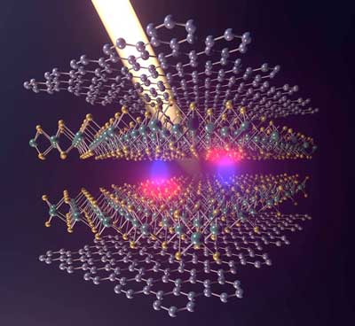 |
| Schematic illustration of the electron-hole pairs (electron: pink, hole: blue), which are formed by absorption of light in the two-layer molybdenum disulfide layer. (Image: Nadine Leisgang and Lorenzo Ceccarelli, Department of Physics, University of Basel) |
| Novel two-dimensional materials are currently a hot research topic around the world. Of special interest are van der Waals heterostructures, which are made up of individual layers of different materials held together by van der Waals forces. The interactions between the different layers can give the resulting material entirely new properties. |
Double layer unlocks crucial properties |
| There are already van der Waals heterostructures that absorb up to 100 percent of light. Single-layers of molybdenum disulfide offer absorption capacities in this range. When light is absorbed, an electron vacates its original position in the valence band, leaving behind a positively charged hole. The electron moves to a higher energy level, known as the conduction band, where it can move freely. |
| The resulting hole and the electron are attracted to each other in accordance with Coulomb’s law, giving rise to bound electron-hole pairs that remain stable at room temperature. However, with single-layer molybdenum disulfide there is no way to control which light wavelengths are absorbed. |
| “It is only when a second layer of molybdenum disulfide is added that we get tunability, an essential property for application purposes,” explains Professor Richard Warburton of the University of Basel’s Department of Physics and Swiss Nanoscience Institute. |
Absorption and tunability |
| Working in close collaboration with researchers in France, Warburton and his team have succeeded in creating such a structure. The physicists used a double layer of molybdenum disulfide sandwiched between an insulator and the electrical conductor graphene on each side. |
| “If we apply a voltage to the outer graphene layers, this generates an electric field that affects the absorption properties of the two molybdenum disulfide layers,” explains Nadine Leisgang, a doctoral student in Warburton’s team and lead author of the study. “By adjusting the voltage applied, we can select the wavelengths at which the electron-hole pairs are formed in these layers.” |
| “This research could pave the way for a new approach to developing optoelectronic devices such as modulators,” adds Richard Warburton. Modulators are used to selectively change a signal’s amplitude. Another potential application is generating individual photons, with important implications for quantum technology. |
| Source: Universität Basel |
|
Subscribe to a free copy of one of our daily Nanowerk Newsletter Email Digests with a compilation of all of the day's news. |

