| Jul 07, 2022 |
New design for plasmonic metasurfaces expands wide-spectrum camera abilities
(Nanowerk News) By turning a traditional lab-based fabrication process upside down, researchers at Duke University have greatly expanded the abilities of light-manipulating metasurfaces while also making them much more robust against the elements.
|
|
The combination could allow these quickly maturing devices to be used in a wide range of practical applications, such as cameras that capture images in a broad spectrum of light in a single shutter snap.
|
|
The results appear in the journal Nano Letters ("Control of Nanoscale Heat Generation with Lithography-Free Metasurface Absorbers").
|
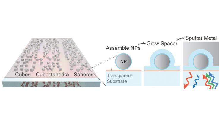 |
| A new upside down fabrication method for light-manipulating metamaterials envelops nanoparticles with a transparent spacing layer followed by a coating of metal. The way the metal coating envelops part of the nanoparticle while maintaining tight, nanometer tolerances allows for a much larger design space than was previously possible. (Image: Duke University)
|
|
Plasmonics is a technology that essentially traps the energy of light in groups of electrons oscillating together on a metal surface. This creates a small but powerful electromagnetic field that interacts with incoming light.
|
|
Traditionally, these groups of electrons — called plasmons — have been excited on the surfaces of metal nanocubes. By controlling the size of the nanocubes and their spacing from each other as well as the metal base below, the system can be tuned to absorb specific wavelengths of light.
|
|
These so-called plasmonic metasurfaces consist of three layers — a metal base coated in a nanometer-thin transparent substrate topped with silver nanocubes. While this configuration has worked well for laboratory demonstrations, it leaves little room for creativity. Because an area of the nanoparticle must be within a few nanometers of the metal surface below, researchers couldn’t use a wide variety of shapes.
|
|
To get around this need for flatness, Maiken Mikkelsen, the James N. and Elizabeth H. Barton Associate Professor of Electrical and Computer Engineering at Duke, and her team decided to try to put each nanoparticle in its own dimple or well. This would surround the entire lower halves of the nanoparticles with metal, allowing the sides to host plasmons as well as the bottoms. But because of incredibly tight tolerances, this is easier said than done.
|
|
“We need to control certain dimensions with single-nanometer precision over the surface of a centimeter-sized wafer,” Mikkelsen said. “That’s like trying to control the thickness of the blades of grass on a football field.”
|
|
To meet this challenge, Mikkelsen and her laboratory essentially flipped the traditional fabrication process upside down. Rather than starting with a metal surface and putting a thin transparent substrate on top followed by nanocubes, they start with the nanocubes, which they cover with a precisely thin spacer coating that follows the underlying shape, and top off with a metal coating. It’s almost like a pineapple upside-down cake, where the nanocubes are the pineapples that get covered in caramelized sugar and baked into a thin bottom.
|
|
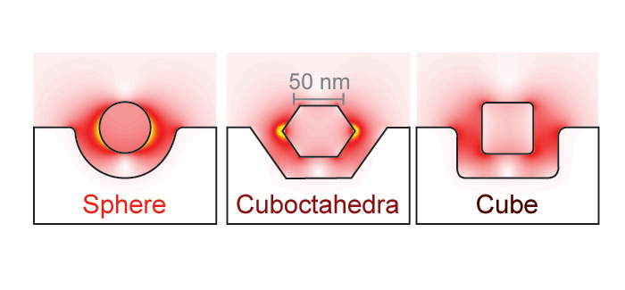
Because more than one surface of the nanocubes could now trap plasmons between gaps, Mikkelsen and her colleagues could experiment in 3D with new nanoparticle shapes. In the paper, the team tried out solid spheres and cuboctahedra — a shape consisting of eight triangular faces and six square faces — as well as metal spheres with a quartz core.
|
 |
| The new upside-down fabrication method allows researchers to use a wide variety of new nanoparticle shapes, such as spheres and cuboctahedra — a shape consisting of eight triangular faces and six square faces. (Image: Duke University)
|
|
“Synthesizing nanoparticles can be tricky and there are limitations for each shape,” Mikkelsen said. “By being able to use almost all shapes, we really open up a lot of new possibilities, including exploring a variety of metals.”
|
|
Test results showed that not only can the new fabrication method match or exceed the capabilities of previous methods using silver nanocubes, it can also expand the range of frequencies that are harnessed by using these different shapes and metals. The research also revealed that these variations change where the nanoparticles capture energy on their surfaces. Combined with the added bonus of essentially weatherizing the entire device by enveloping the nanoparticles, the new technique could potentially expand the technology’s use into driving chemical reactions or thermal detectors.
|
|
Mikkelsen’s first priority, however, is applying the fabrication technique to her $7.5 million Department of Defense project to create a “super camera” that can capture and process a wide range of light’s properties, such as polarization, depth, phase, coherence and incidence angle.
|
|
“What is really significant here, is that large, macroscopic areas can be covered by the metasurfaces very inexpensively, as we use entirely lithography-free fabrication techniques,” Mikkelsen said. “This means the metasurfaces can be integrated with other existing technologies and also create inspiration for new plasmonic metasurface applications.”
|

