| Jul 02, 2025 |
Ultrafast laser nanofabrication advances manufacturing limitsAdvanced ultrafast laser techniques achieve sub-10nm nanofabrication for semiconductors. Comprehensive review of near-field and far-field approaches.(Nanowerk News) Nanofabrication continues to evolve as engineers work to increase component density and performance across chip manufacturing, nanophotonics, and quantum devices. The push for smaller feature sizes drives ongoing innovation in material processing techniques. |
| A recent article in Engineering ("Advancing Manufacturing Limits: Ultrafast Laser Nanofabrication Techniques") by Zhenyuan Lin, Lingfei Ji, and Minghui Hong examines current developments in ultrafast laser nanofabrication, covering both near-field and far-field laser techniques while addressing remaining technical challenges. |
 |
| ASOM: adaptive scanning optical microscope. (Image: Zhenyuan Lin, Lingfei Ji, Minghui Hong) |
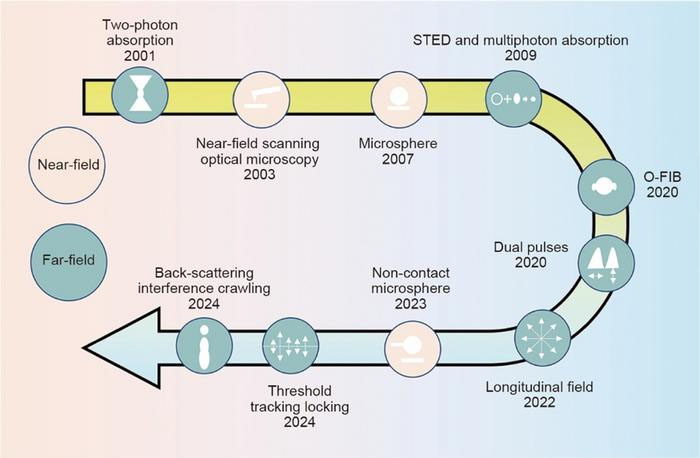
| Current nanofabrication methods like electron beam lithography and nanoimprint lithography routinely achieve resolutions in the tens of nanometers range. However, the semiconductor industry's progression toward 3 nm process technology and planned 2 nm processes requires further advances in manufacturing capabilities. While lasers have been available since 1960 and show promise for maskless nanolithography and direct 3D writing, nanopatterning beyond the optical diffraction limit in far-field atmospheric environments presents significant technical hurdles. |
| Near-field laser nanomanufacturing manipulates optical fields through discontinuous interfaces at nanoscale dimensions. This approach utilizes evanescent waves and has demonstrated the capability to produce nanostructures with feature sizes as small as 11 nm. The technique faces practical limitations, though, including short working distances and sensitivity to surface disturbances that complicate large-scale implementation. Researchers have integrated precision controls such as optical tweezers and atomic force microscopy to improve resolution and extend working distances. |
| Far-field laser nanomanufacturing offers simpler optical configurations and broader material compatibility, making it more suitable for industrial production. While constrained by diffraction limits, recent advances in techniques like stimulated emission depletion (STED), multiphoton absorption, and optical far-field-induced near-field enhancement have achieved feature sizes in the tens of nanometers. STED has produced 3D nanoengravings with minimum dimensions around 55 nm, while multiphoton absorption using femtosecond lasers has reached 26 nm feature sizes. |
| Several innovative approaches have pushed far-field laser nanofabrication boundaries further. Dual-beam overlapping and backscattering interference techniques show potential for sub-10 nm features. Dual 405 nm nanosecond laser overlapping has achieved minimum linewidths of 5 nm, and dual orthogonal polarization overlapping with 800 nm femtosecond lasers has enabled 12 nm nanostructure fabrication on silicon surfaces. |
| Despite these advances, several challenges persist. Achieving nanometric high-aspect-ratio processing remains difficult because diffraction-limited light propagation conflicts with requirements for uniform axial and subwavelength lateral energy deposition. The instability of nonlinear threshold phenomena also limits processing sizes to approximately 10 nm. Researchers are exploring solutions including axially stretched or multifocus beam irradiation and dicing technologies based on Bessel–Gaussian beams. |
| The work highlights substantial progress in ultrafast laser nanofabrication while noting areas requiring additional research. Development of new laser sources, pulse-shaping technologies, and parallel beam manufacturing techniques may enable high-resolution, high-efficiency, large-scale nanofabrication. As semiconductor manufacturing moves toward smaller and more complex devices, advances in ultrafast laser nanofabrication will likely play an important role in future nanotechnology development. |
| Source: Higher Education Press (Note: Content may be edited for style and length) |

