| Aug 04, 2025 |
Double-layer grapene membranes lead to ultra-small, high-yield motion sensorsA new graphene-based accelerometer design improves durability and yield using 1 micron trenches, offering potential for wearables, robotics, and medical devices.(Nanowerk News) Researchers from the Beijing Institute of Technology and North University of China have developed a compact accelerometer using suspended graphene membranes, designed to offer greater mechanical stability and higher manufacturing yield. The sensor, part of a class of anoelectromechanical systems (NEMS), uses a double-layer graphene structure paired with a silicon-based proof mass. |
| Graphene has strong potential for motion sensing, but its use in accelerometers has been limited. One of the main design challenges is integrating an atomically thin membrane with a small mass while maintaining structural strength and ease of fabrication. Many earlier designs used relatively wide trenches—2 to 4 micrometers—to suspend graphene. These wider structures often suffered from low yield and durability during production. |
| The new approach, published in Microsystems & Nanoengineering ("Suspended graphene-based NEMS accelerometers with direct electrical readout"), uses 1 μm-wide trenches to suspend a double-layer graphene membrane. This narrower design, combined with an attached SiO₂/Si proof mass, improves mechanical performance and increases device yield to 90%. The study tested three versions of the sensor under acceleration up to 2 g at 160 Hz. Smaller proof masses resulted in higher sensitivity, while wider trenches produced stronger signals but with reduced stability. |
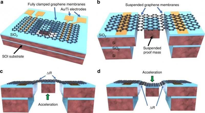 |
| Schematic diagrams of graphene NEMS accelerometers. a 3D schematic of the proposed graphene NEMS accelerometer. b 3D schematic of the cross-section of the graphene NEMS accelerometer. c, d Schematics of working principle of the graphene NEMS accelerometer. (Image: CAS) |
| Mechanical tests using atomic force microscopy and simulations showed the devices could withstand extreme loads without failure. Long-term testing confirmed electrical stability over six months of use. |
| The fabrication process is compatible with standard semiconductor techniques, including thermal oxidation, trench etching, and graphene transfer. This supports scalability and integration into existing electronics manufacturing. The design highlights trade-offs between trench width, proof mass, and overall performance, offering options for tailoring the sensor to specific applications. |
| “These results show how modifying the membrane structure and support geometry can improve both performance and manufacturing efficiency,” said Prof. Xuge Fan, who led the study. He noted that the 1 μm trench width supports consistent performance while remaining suitable for large-scale production. |
| Potential applications include wearable health monitors, implantable devices, precision robotics, and other areas where small, durable sensors are needed. Future work will look at integrating wireless functions and expanding to multi-axis sensing. |
| Source: Chinese Academy of Sciences (Note: Content may be edited for style and length) |

