| Posted: May 09, 2018 |
Studying strain effects in 2D materials using Kelvin Probe Microcopy |
| (Nanowerk Spotlight) Inspired by the unique optical and electronic property of graphene, two-dimensional (2D) layered materials have been intensively investigated in recent years, driven by their potential applications for nanoelectronics, in particular in flexible and wearable technologies. |
| At the nanoscale, materials become exceedingly sensitive to external perturbations. This is quite a relevant factor for wearable and flexible applications, where materials would always bear a certain degree of variable strain/stress. |
| "Effects of strain can be significant, for example some materials can transform from being semi-conductors to metallic with strain," Syed Ghazi Sarwat, a PhD candidate in Harish Bhaskaran's group at Oxford University, tells Nanowerk. "This can be quite frustrating as a device could completely lose its functionality. However, strain can also be exploited, for instance in catalysis or in making field effect strain sensors." |
| However, so far it has been very difficult to characterize strain effects in 2D materials, which is crucial to understanding strain-matter interactions. |
| Conventionally, strain in materials is studied using optical spectroscopy. While being a robust approach, this technique is generally limited to the microscale and to materials that have direct band-gaps. |
| That means that graphene, which has zero band gap, and many other materials that have indirect band-gaps, cannot be studied for strain effects. Furthermore, flexible substrates on which 2D materials reside can mask the strain effects. |
| In a new paper in Nano Letters ("Revealing Strain-Induced Effects in Ultrathin Heterostructures at the Nanoscale"), first-authored by Sarwat, the Bhaskaran Group demonstrates that this limitation can be overcome by using a technique based on Kelvin Probe Microcopy. |
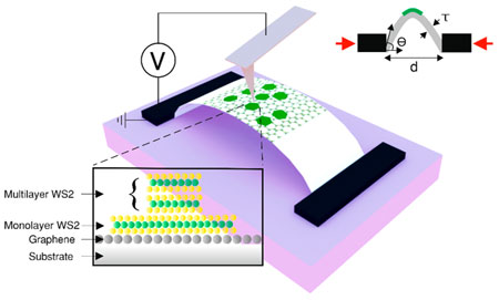 |
| A schematic illustration of the strain characterization setup. Top right inset is a schematic of the two-point bending apparatus. The strain is estimated using the equation ε = τ × sin θ/d. Bottom left inset illustrates the heterostructure consisting graphene/WS2 monolayer/WS2 multilayer. (Reprinted with permission by American Chemical Society) |
| In this work, the team reveals strain induced modulation in ultrathin 2D materials' heterostructures. These materials are being intensively pursued for next-generation electronic and optoelectronic devices. |
| "We show that strain can strongly modulate the electronic energy landscape (energy band diagrams) of the heterostructures, which can surprisingly also result in the materials to behave differently as would be expected in their isolated forms," explains Sarwat. "We also find that the junctions that form at the interfaces between the materials get modulated from strain as well." |
| As an example, he notes that if such a heterostructure was to be used as an LED, strain alone could cause fluctuations in the illumination intensity, perhaps even blank it out. |
| Sarwat emphasizes that the team's results can aid any study that requires realization of strain modulation in individual components with a nanoscale resolution in a multicomponent system and in the study of spatial strain distribution in a homogeneous system. They are also important for the practical aspects of device engineering. |
| Next in their investigations, the researchers aim to use atomic-scale, as well as finite element modeling to verify the nature of band-alignment and strain transfer, and possibly even harness strain modulation in devices such as gas and chemical sensors. |
 By
Michael
Berger
– Michael is author of four books by the Royal Society of Chemistry:
Nano-Society: Pushing the Boundaries of Technology (2009),
Nanotechnology: The Future is Tiny (2016),
Nanoengineering: The Skills and Tools Making Technology Invisible (2019), and
Waste not! How Nanotechnologies Can Increase Efficiencies Throughout Society (2025)
Copyright ©
Nanowerk LLC
By
Michael
Berger
– Michael is author of four books by the Royal Society of Chemistry:
Nano-Society: Pushing the Boundaries of Technology (2009),
Nanotechnology: The Future is Tiny (2016),
Nanoengineering: The Skills and Tools Making Technology Invisible (2019), and
Waste not! How Nanotechnologies Can Increase Efficiencies Throughout Society (2025)
Copyright ©
Nanowerk LLC
|

Become a Spotlight guest author! Join our large and growing group of guest contributors. Have you just published a scientific paper or have other exciting developments to share with the nanotechnology community? Here is how to publish on nanowerk.com. |
