Showing Spotlights 345 - 352 of 627 in category All (newest first):
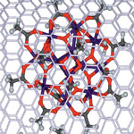 Single-molecule magnets (SMM) are fascinating nanoscale structures with unique functional properties showing promise for high-density electronic data storage devices, solid state quantum computers, spintronic devices such as spin valves, and other advanced technological applications. Despite a flurry of research in this area - since an individual magnetic molecule represents the ultimate size limit to storing and processing information - the main challenge related to harnessing properties of SMM remained unsolved. A new study by a group of European researchers reports the successful encapsulation of single-molecule magnets in carbon nanotubes, yielding a new type of hybrid nanostructure that combines all the key single-molecule magnet properties of the guest molecules with the functional properties of the host CNT.
Jul 27th, 2011
 To build microprocessors with more than one billion transistors, manufacturers still use the same technique - photolithography, the high-tech, nanoscale version of printing technology - that they have been using for the past 50 years. State-of-the-art photolithography processes use 193 nm light to produce diffraction-limited features as small as 32 nm. Going beyond 32 nm, the cost and complexity rises significantly, posing massive technological and economic challenges for chip manufacturers. This provides plenty of incentives for researchers to explore alternative manufacturing technologies for chipmakers. One novel approach is based on the use of DNA nanostructures to pattern a silicon wafer.
Jul 26th, 2011
 For more than 5000 years, noble metals have been known to be impervious to magnetic fields. Significant scientific breakthroughs in the recent past have led to making either 13 atoms clusters of platinum or organic molecule capped noble metal nanoparticles magnetic. By carefully controlling the size, shape, and composition of noble metals - especially in confined nanoscale systems - their properties can be modified, potentially leading to significantly advanced nanomaterial-based applications such as catalysis, self-assembly, novel metamaterials, improved MRI research, and spintronics. Now, researchers have developed simple method to make nano- and macro-particles of noble metals magnetic.
Jul 12th, 2011
 It is not often that the prefix multipliers kilo and nano come together, and when they do, it usually is in the opening chapters of physical sciences textbooks where the point is made that the universe around us spans enormous space and time scales while operating in unimaginably small ones. We are truly awestruck and inspired by the tension. Kilometer-long nanowires do have a similar eponymous echo. Researchers have now reported the first successful fabrication of arrays of millions of ordered indefinitely long nanowires and nanotubes in a flexible polymer fiber. The results are kilometer-long nanowires - a novel approach to nanowire fabrication that might bring with it fresh solutions.
Jun 23rd, 2011
 Radiation damage to materials is a major issue for builders of nuclear power plants as well as spacecraft engineers. The former have to worry about material failure due to the destructive radiation created within the reactor; the later are concerned about the exposure to space radiation of both materials and humans during long-term space missions. There is a consensus that interface engineering is the way to go to to improve resistance to extreme conditions in general and to reach radiation tolerance in particular - interfaces are places where defects created by energetic collision in solids can annihilate each other and thus render the material immune to irradiation. All kind of interfaces are being explored, in particular those formed by the contact between two different solid state phases.
Jun 15th, 2011
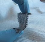 The future of your shirts, socks and gloves will be electronic. In years to come, wearable electronics will look nothing like even your smallest iPod or mobile phone today. Not only will such devices be embedded on textile substrates, but an electronics device or system could become the fabric itself. Here is some recent work that demonstrates the kind of issues scientists are working on today and that will help improve the performance of electronic textile structures. Using atomic layer deposition (ALD), researchers have grown coatings of inorganic materials on the surface of textiles like woven cotton and nonwoven polypropylene. By fabricating an all-fiber capacitor, they show that their coated materials are sufficiently conductive to perform in simple device architectures.
Jun 9th, 2011
 The small particles in volcanic ash can damage jet aircraft engines. During jet engine operation, large amounts of air are sucked in. If this air contains ash particles, especially glass-rich silicate ash, they will melt in the jet turbine's operating temperature of 1400-1500C and subsequently fuse to the turbine blades. This will drive the finely tuned blades out-of-balance and could stall the engine. In today's jet engines, a thermal barrier coating (TBC) insulates metallic engine parts from the heat generated by the combustion process. If ingested ash melts onto this coating it will penetrate it and, upon cooling, the molten ash forms a brittle glass that flakes off, taking the coating with it. A team of researchers have now examined a new class of ceramic TBC that could offer jet engines special protection against volcanic ash damage in the future.
May 31st, 2011
 Microfluidic chips have proven to be a breakthrough analytical technique that has rendered analysis of proteins a medical routine. The sensitivity limits of immunoassays have been enhanced to picomolar concentrations using monoclonal antibodies, new labeling techniques, and devices for signal transduction and acquisition. It is now possible to routinely determine levels of hormones, cancer markers, response to infection with bacteria and viruses, monitor the evolution of a disease and test for medication levels. In a new review article, researchers argue that the most promising opportunities of microfluidics for diagnostics reside in point-of-care applications because a number of unmet needs can be fulfilled by microfluidic devices due to their portability, short sample processing time, and flexibility.
May 17th, 2011
 Subscribe to our Nanotechnology Spotlight feed