Showing Spotlights 697 - 704 of 2786 in category All (newest first):
 Despite the rise of graphene and other two-dimensional (2-D) materials, semiconducting single-walled carbon nanotubes are still regarded as strong candidates for the next generation of high-performance, ultra-scaled and thin-film transistors as well as for opto-electronic devices. In new work, a European team of researchers demonstrates simultaneous confinement of electrons and holes between artificial defects separated by less than 10 nm in semiconducting carbon nanotubes.
Mar 16th, 2018
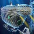
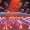
 Scientists have discovered that cell sex is an important overlooked factor at the nanobio interfaces. More specifically, depending on their sex, cells respond differently to the exact same type of nanoparticles. These findings have a capacity to optimize clinical translation of nanoparticles and also to help researchers to better design and produce safe and efficient therapeutic sex-specific nanoparticles. It is likely that there are other undiscovered differences that could influence nanoparticle uptake.
Mar 15th, 2018
 Single- or few-layer black phosphorus (BP) is one of the most promising two-dimensional semiconductors for electronic and optoelectronic device applications but its environmental instability has always posed a major hurdle for BP-based devices. In contrast, black phosphorus analogues (BPA) nanoarchitectures not only own the similar folded structure of BP, its tunable bandgap energy band and high carrier mobility, but exhibit excellent environmental stability as well. BPA nanosheets can be fabricated by a facile liquid-phase exfoliation method.
Mar 14th, 2018
 Given the vast, and still rising, cost of optical lithography tools, researchers have considered alternative patterning technologies such as electron beam lithography (EBL), and nanoimprint technology (NIL) in order to enable the manufacturing of next-generation integrated circuits, flash memory, and hard disk drives. Now that the length scales attainable by top-down lithography are approaching that of bottom-up self-assembly found in polymers and small molecules, scientists are increasingly looking at bottom-up patterning technologies based on self-assembly.
Mar 9th, 2018
 Due to its fascinating properties, black phosphorus (BP) has demonstrated appealing potential for not only building (opto)electronic devices, but also in many other areas such as lithium-ion batteries, solar cells, sensors, thermoelectric devices, supercapacitors, and phototherapy. Researchers now have demonstrated that modifying BP with metal ions solved its previous instability problem, which hindered the practical application of BP in electronics and optoelectronics; while at the same time further enhancing the original superior transport properties.
Mar 7th, 2018
 Enzymatic biofuel cells (EBFCs) are bioelectronic devices that utilize enzymes as the electrocatalysts to catalyze the oxidation of fuel and/or the reduction of oxygen or peroxide for energy conversion to electricity. EBFCs have already been demonstrated as wearable epidermal tattoo biosensors and in new work, researchers report the fabrication flexible EBFCs with flexible nanoporous gold electrodes that were modified with lactate oxidase and bilirubin oxidase for use as a lactate/O2 biofuel cell.
Mar 6th, 2018
 For the first time, liquid-phase exfoliation (LPE) - a widely explored technique to obtain two-dimensional (2D) layered nano-architectures - has been successfully used to exfoliate tellurium, a non-layered material. The resulting 2D Te nanosheets exhibit excellent photoresponse behavior from the UV to the visible regime in association with strong time and cycle stability for on/off switching behavior. This intriguing finding could help in the search for other 2D materials for innovative applications.
Mar 5th, 2018
 Recently, a new member has been introduced to the family of two-dimensional (2D) materials: phosphorene. Phosphorene has attracted much attention because of its tunable direct band gap and superior carrier mobility, but unfortunately phosphorene is subjected to oxidation and degradation under ambient conditions. Now, researchers have reported a facile pathway in obtaining and stabilizing phosphorene through a one-step, ionic liquid-assisted electrochemical exfoliation and synchronous fluorination process. This strategy enabled a novel phosphorene derivative to be discovered - fluorinated phosphorene, which exhibits air-stable photo-thermal properties.
Mar 2nd, 2018
 Subscribe to our Nanotechnology Spotlight feed