| Posted: Mar 09, 2018 |
Nanopatterning below 5 nm - towards the design of molecular building blocks |
| (Nanowerk Spotlight) Photolithography, the standard workhorse employed in today's semiconductor industry, has been the driver behind the ability to print increasingly smaller features at a lower cost. In order to facilitate the production of even smaller features, extreme-UV (EUV) lithography, utilizing radiation of wavelength 13.5 nm, is currently being pursued on a global scale, even though it is tremendously complex and expensive (read more: "The long and tortuous path of EUV lithography to full production"). |
| Given the vast, and still rising, cost of optical lithography tools, researchers have considered alternative patterning technologies such as electron beam lithography (EBL), and nanoimprint technology (NIL) in order to enable the manufacturing of next-generation integrated circuits, flash memory, and hard disk drives. |
| Now that the length scales attainable by top-down lithography are approaching that of bottom-up self-assembly found in polymers and small molecules, scientists are increasingly looking at bottom-up patterning technologies based on self-assembly. |
| The utilization of organic building blocks as self-assembled etch masks is particularly attractive since the lithographic information is contained in the self-assembling material itself, rather than provided in an exposure step. |
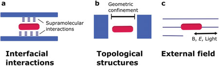 |
| Schematic representation of directed self-assembly of liquid-crystalline small molecules, involving a) tailored interfacial interactions, b) topologically structured interfaces, and c) external fields. (Reprinted with permission by Wiley-VCH Verlag) |
| A recent review article in Advanced Materials ("Directed Self-Assembly of Liquid-Crystalline Molecular Building Blocks for Sub-5 nm Nanopatterning") by Koen Nickmans and Albert P. H. J. Schenning from Eindhoven University of Technology, discusses various organic building blocks for sub-5 nm patterning and their use in the fabrication of inorganic sub-5 nm patterns. |
| Specifically, they address these building blocks: |
|
|
| and these fabrication methods: |
|
|
| The authors note that with respect to feature sizes, the sub-5 nm features reported in their article are far ahead of the scaling curve pursued by the semiconductor industry. "This observation implies that several critical challenges must be overcome for these materials to be integrated into existing patterning technologies. Most notably, the critical challenges are related to the development of suitable pattern transfer techniques, mechanical stability of the ultrafine features, the application of appropriate metrology tools, and the integration of the required processing operations into fabrication facilities." |
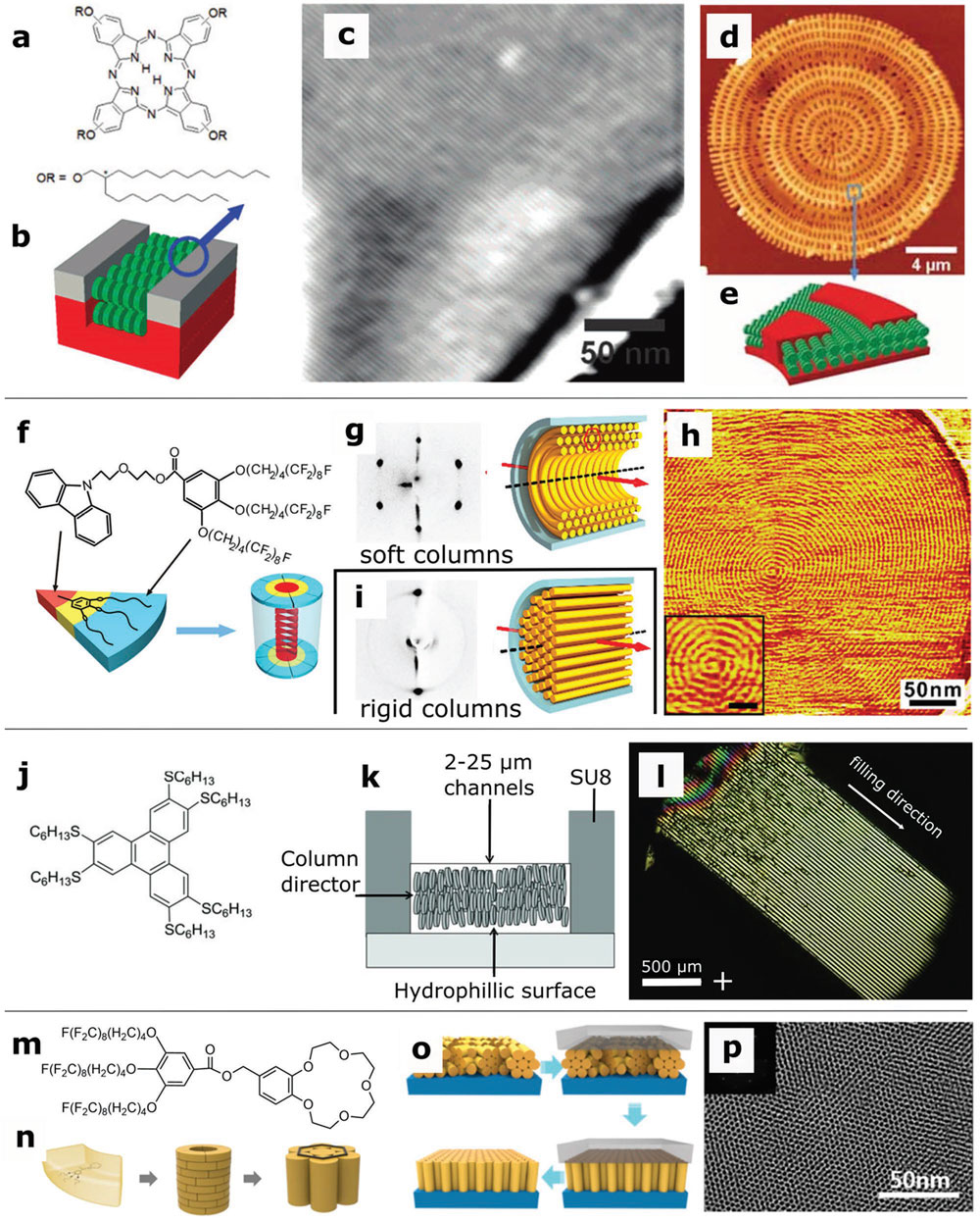 |
| Directed self-assembly of sub-5 nm patterns for organic electronics. a?c) In-plane alignment of a tetrasubstituted phthalocyanine in topological guiding structures of 200 nm width. d,e) Alignment of (a) in a tangentially aligned spiral network. f?h) Circular alignment of a soft dendronized carbazole (f) in 400 nm circular anodized alumina pore showing extremely high curvature (bar in inset = 8 nm). i) In the case of rigid LCs, axial rather than circular alignment is generated. j?l) In-plane alignment of substituted triphenylene (j) in SU8 microchannels. l) POM image of (j) in 10-µm-wide SU8 channels. The cross represents the polarizer axes. The arrow indicates the filling direction. m) Perfluorinated tapered monodendron, n) cylindrical dendrimers formed by (m) with 4.5 nm lattice spacing. o) Soft confinement protocol. p) TEM image after annealing a thin film of dendrimer (m) between a carbon bottom (carbon-supported TEM grid) and a PDMS top surface while cooling from the isotropic transition temperature (78 ?C) to room temperature at a rate of 0.1°C min-1. (© Wiley; " ACS) (click on image to enlarge) |
| They go on to discuss the challenges and bottlenecks that are facing the industry: integration; pattern transfer; defect density and alignment; and metrology. |
| "Recent advances in precise morphological control present unique opportunities for obtaining highly ordered, hybrid organic/inorganic sub-5 nm nanostructured morphologies," the authors conclude. "Coupled with directed self-assembly for 3D orientational control and large-area alignment, this exciting class of materials could lead to a broad range of impending nanotechnologies, most notably nanopatterning. Given the impact of these technologies, it is foreseeable that this thrilling field will continue to expand at a rapid pace." |
 By
Michael
Berger
– Michael is author of four books by the Royal Society of Chemistry:
Nano-Society: Pushing the Boundaries of Technology (2009),
Nanotechnology: The Future is Tiny (2016),
Nanoengineering: The Skills and Tools Making Technology Invisible (2019), and
Waste not! How Nanotechnologies Can Increase Efficiencies Throughout Society (2025)
Copyright ©
Nanowerk LLC
By
Michael
Berger
– Michael is author of four books by the Royal Society of Chemistry:
Nano-Society: Pushing the Boundaries of Technology (2009),
Nanotechnology: The Future is Tiny (2016),
Nanoengineering: The Skills and Tools Making Technology Invisible (2019), and
Waste not! How Nanotechnologies Can Increase Efficiencies Throughout Society (2025)
Copyright ©
Nanowerk LLC
|

Become a Spotlight guest author! Join our large and growing group of guest contributors. Have you just published a scientific paper or have other exciting developments to share with the nanotechnology community? Here is how to publish on nanowerk.com. |
