| Posted: Oct 08, 2009 | |
Scanning thermal microscopy |
|
| (Nanowerk Spotlight) Today, in our Application Note series, we are covering Scanning Thermal Microscopy (SThM) – an atomic force microscopy (AFM) imaging mode that maps changes in thermal conductivity across a sample's surface. | |
| Similar to other modes that measure material properties, SThM data is acquired simultaneously with topographic data. The SThM mode is made possible by replacing the standard contact mode cantilever with a nanofabricated thermal probe with a resistive element near the apex of the probe tip. This resistor is incorporated into one leg of a Wheatstone bridge circuit, which allows the system to monitor resistance. This resistance correlates with temperature at the end of the probe, and the Wheatstone bridge may be configured to either monitor the temperature of a sample or to qualitatively map the thermal conductivity of the sample. | |
  |
|
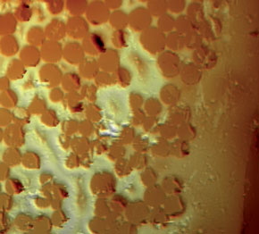
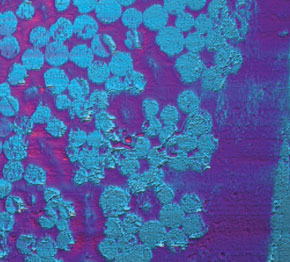
| Figure 1: Imaging of a carbon fiber and epoxy sample. (Top) Topography image. Z-range corresponds to 1.4 µm. (Bottom) SThM image. Z-range corresponds to 600 mV. The XY-range of both images corresponds to 80 µm x 90 µm. | |
| Changes in sample temperatures are often measured on active device structures. For example, it is possible to image hot spots and temperature gradients on devices such as magnetic recording heads, laser diodes, and electrical circuits. | |
| Thermal conductivity imaging, however, is commonly applied to composite or blended samples. In this mode, a voltage is applied to the probe and a feedback loop is used to keep the probe at a constant temperature. As the thermal probe is scanned across the sample surface, more or less energy will be drained from the tip as it scans across different materials. If the region is one of high thermal conductivity, more energy will flow away from the tip. When this occurs, the thermal feedback loop will adjust the voltage to the probe to keep it at a constant temperature. When the probe moves to an area of lower thermal conductivity, the feedback loop will lower the voltage to the probe, as it will require less energy to keep the probe at a constant temperature. By adjusting the voltage to keep the probe temperature constant, a map of the sample’s thermal conductivity is generated. | |
| Figure 2 below displays simultaneously acquired Static Mode Topography and SThM images of a carbon fiber and epoxy sample. The sample has been cross-sectioned and polished to provide a flat surface. | |
 |
|
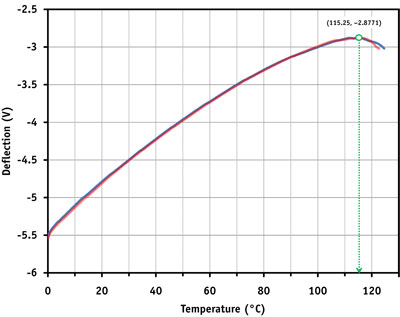
| Figure 2: Local nano-TA analysis of a poly-ethylene film. Graph showing measurement results that were performed at two individual sample sites (blue and red curves, respectively). The onset of melting occurs at 115°C. | |
| Having a smooth surface will minimize changes in the SThM contrast that result from topographic effects. In the SThM image here, it is possible to map the thermal conductivity difference of the epoxy regions and the carbon fibers. As expected, the carbon fibers are seen to have a higher thermal conductivity (light blue) than the surrounding epoxy regions (purple). These data also serve to verify the sub-100-nm resolution that is expected from the thermal probes. | |
| Beyond adding the extended capabilities of SThM imaging, it is also possible to acquire local quantitative thermo-mechanical information with sub-100-nm resolution. | |
| Once an area of thermal interest has been identified using standard Topography imaging with the thermal probe, it is then possible to place the probe at a specific point to measure local thermal properties. This information is obtained by linearly ramping the temperature of the nano-TA probe with time while monitoring deflection of the probe. The thermo-mechanical response allows the user to obtain quantitative measurements of phase transition temperatures such as melting point (Tm) and glass transition temperatures (Tg). At the point of these phase transition temperatures, the sample beneath the probe will soften, allowing the probe to penetrate into the sample. | |
| As seen in Figure 2, this produces a plot of probe deflection as a function of temperature. This breakthrough in spatial resolution of thermal properties has significant implications in the fields of polymer science and pharmaceuticals where understanding local thermal behavior is crucial. | |
| System Requirements | |
| In the experiments described here, hardware and software from Anasys Instruments were used (the Anasys GLA-1 and AN2-200 thermal probes), integrated with the FlexAFM system from Nanosurf easyScan FlexAFM with Signal Module A and Cantilever Holder ST). | |
| The Anasys SThM system includes a simple software interface that controls the thermal analysis electronics via a USB connection. This interface is capable of outputting a low-noise, high-resolution voltage to the probe. The voltage may be varied over a wide range depending on the probe type and the desired temperature of the probe (<0.1°C resolution). | |
| The other components in the bridge circuit are easily changed if required for custom experiments, and the system includes an input connection to apply AC voltages to the probe. The resistance of the probe is output on a BNC, which is then connected to User Input 1 on the easyScan 2 Signal Module A. | |
| For SThM imaging, the easyScan 2 control software is configured to collect the resistance data on User Input 1, allowing SThM information to be recorded and displayed as a chart in the imaging window of the Nanosurf software. During nano-TA experiments, the Anasys software allows the User to set Nano-TA2 controller parameters such as heating rates and temperature range. Typically, AFM feedback is turned off during the acquisition of nano-TA data. | |
|
Become a Spotlight guest author! Join our large and growing group of guest contributors. Have you just published a scientific paper or have other exciting developments to share with the nanotechnology community? Here is how to publish on nanowerk.com. |
|