| Posted: Oct 12, 2009 | |
Nanoengineered thin films lead to novel plasmonic modes |
|
| (Nanowerk Spotlight) Surface-plasmon resonance is a quantum-electromagnetic phenomenon arising from the interaction of light with free electrons at the planar interface of a metal and a (nonconducting) dielectric material. This resonance arises when the energy carried by photons in the dielectric material is transferred to collective excitations (called plasmons) of free electrons in the metal at that interface. As the free electrons in the metal are coupled to the photons in the polarizable dielectric material, the quantum is called a surface plasmon-polariton (SPP). | |
| These electromagnetic SPP waves have become a popular topic in contemporary research. Proposed uses include plasmonic circuits to make ultrafast computers, plasmonics-based invisibility cloaks, and highly efficient light-emitting diodes. Extremely sensitive chemical and biochemical detection systems and imaging systems have already been demonstrated. | |
| Research on SPP-wave-based chemical and biochemical detection systems in particular has flourished for over two decades. Species such as pesticides, explosives, environmental pollutants, bacteria, viruses, toxins, allergens, and biomedical analytes have been detected. Researchers remain focused on various means of exciting and detecting the SPP wave, binding of recognition molecules to the interface for detecting biomaterials, and incorporating surrounding structures to modify the SPP wave. | |
| Typically, a SPP wave is launched on a metal-dielectric interface at one particular frequency. That wave has a certain polarization state. Researchers have now shown theoretically and experimentally that by modifying the dielectric material, novel surface-plasmon-polariton wave behavior can be created with the result that the same interface can independently guide more than one SPP wave. Although propagating at the same frequency, these waves can have different speeds and polarization states. This will allow selective excitation and detection, enabling new applications of SPP waves. | |
| To achieve this result, the scientists used a nonhomogeneous dielectric material whose periodic nonhomogeneity is nanoengineered. This particular type of material is called a sculptured thin film (STF). | |
| "The impact on many technologies of these developments would be significant," Akhlesh Lakhtakia, the Charles Godfrey Binder Professor of Engineering Science and Mechanics at Penn State University, tells Nanowerk. "Different SPP waves would have different configurations of electromagnetic fields, phase speeds, and attenuation rates. For sensing applications, the use of more than one SPP waves would increase confidence in the reported measurement; also, more than one analyte could be sensed at the same time, thereby increasing the capabilities of multi-analyte sensors. For imaging applications, the simultaneous creation of two images may become possible. For plasmonic communications, the availability of multiple channels would make information transmission more reliable as well as with increased capacity." | |
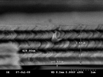
| Lakhtakia and his team examined two types of STFs for exciting SPP waves: sculptured nematic thin films (SNTFs) and chiral STFs, both made of an inorganic material (the metal film is aluminum with a thickness of 15nm). An STF is an electromagnetically complex medium because it is nonhomogeneous along the direction normal to the planar interface, and it is optically biaxial since, in general, the cross-sections of the nanocolumns are elliptical. | |
 |
|
| SEM image of a chiral STF of magnesium fluoride. (Image: Dr. Akhlesh Lakhtakia, Penn State) | |
| "SNTFs are produced by rocking the substrate to produce slanted wavy nanocolumns with essentially 2D morphology, while chiral STFs are produced by rotating the substrate about its normal to produce helical nanocolumns with 3D morphology," explains Lakhtakia. "In addition to functioning simply as the dielectric side of the interface along which the SPP travels, an STF may have an advantage over dense dielectric materials in certain applications because of its tailorable porosity. In detector applications, STFs may allow analytes to infiltrate very close to the interface for very sensitive detection and, at the same time, filter out larger undesirable particles." | |
| Lakhtakia points out that novel SPP wave behavior other than what he and his team have described so far may yet be discovered with consideration of other forms of STF periodicity, different STF materials, and various metals. | |
| "We plan to intensively study the role of STF morphology in the multiplicity of modes of SPP wave propagation, with an eye toward practical feasibility. Simultaneously, we will experimentally establish that the periodic nonhomogeneity of many STFs does indeed engender that multiplicity." | |
| The theoretical and experimental work behind these findings has been published, in part, in a series of three papers in the Journal of Nanophotonics: | |
| "Multiple trains of same-color surface plasmon-polaritons guided by the planar interface of a metal and a sculptured nematic thin film". | |
| "Multiple trains of same-color surface plasmon-polaritons guided by the planar interface of a metal and a sculptured nematic thin film. Part II: Arbitrary incidence". | |
| "Multiple trains of same-color surface plasmon-polaritons guided by the planar interface of a metal and a sculptured nematic thin film. Part III: Experimental evidence". | |
 By
Michael
Berger
– Michael is author of three books by the Royal Society of Chemistry:
Nano-Society: Pushing the Boundaries of Technology,
Nanotechnology: The Future is Tiny, and
Nanoengineering: The Skills and Tools Making Technology Invisible
Copyright ©
Nanowerk LLC
By
Michael
Berger
– Michael is author of three books by the Royal Society of Chemistry:
Nano-Society: Pushing the Boundaries of Technology,
Nanotechnology: The Future is Tiny, and
Nanoengineering: The Skills and Tools Making Technology Invisible
Copyright ©
Nanowerk LLC
|
|
|
Become a Spotlight guest author! Join our large and growing group of guest contributors. Have you just published a scientific paper or have other exciting developments to share with the nanotechnology community? Here is how to publish on nanowerk.com. |
|