| Posted: Jul 22, 2014 | |
How nanostructure geometry affects polymer photovoltaic device efficiency |
|
| (Nanowerk Spotlight) Conjugated polymer based organic photovoltaic (OPV) devices have been the subject of increasing research interest over the past years due to their potential of being light weight, mechanically flexible, semitransparent. However, the highest power conversion efficiency (PCE) achieved by this type of solar cell is still lower than their inorganic counterparts (currently about 7-8% compared to >10%). | |
| To increase the efficiency of OPV, it is necessary to achieve a precisely controlled donor-acceptor phase separation within the short exciton diffusion length (∼10 nm) without dead ends, as well as a high hole mobility within the polymer. | |
| So far, it has been impossible to achieve such a morphology in the most widely used bulk heterojunction structure in which randomly distributed phases cause significant charge recombination. | |
| Nanoimprint lithography (NIL) has emerged as an effective fabrication technique to precisely control the nanoscale morphology of this type of solar cells and new work shows that it is an effective technique to solve these issues simultaneously. | |
| Generally, three fabrication methods have been used to fabricate nanoimprinted organic photovoltaics: spin-coating, physical vapor deposition, and lamination. Most nanoimprinted OPVs have architectures where fullerene acceptors are infiltrated into nanoimprinted, semicrystalline polymer nanostructures after a controlled chain ordering as well as a bicontinuous and interdigitized heterojunction has been realized. | |
| In a previous Nanowerk Spotlight, we covered a review paper on the state of nanoimprinted polymer organic solar cell technology. One of its conclusions was that, despite the significant progress made in the field, a fundamental understanding of the nanostructure geometry effects on the polymer chain alignment and OPV performance remains largely unknown. | |
| The authors attributed this gap in understanding to the inconsistent geometries of the imprinted polymer nanostructures used by different research groups, which result in different sizes and shapes of donor/acceptor junctions as well as differently oriented polymer chain alignments which in turn affect the device performance. They concluded that this makes it difficult to compare the results reported in the literature. | |
| Now, in a new paper recently published in Nanoscale ("Effects of nanostructure geometry on nanoimprinted polymer photovoltaics"), the authors of this review paper – led by Walter Hu, an Associate Professor of Electrical Engineering, and Anvar Zakhidov, a professor of physics, both at UT Dallas – have proven that these contradicting results can be explained by the effects of nanostructure geometry, i.e., that different geometries result in different chain orientations and thus device efficiencies. | |
 |
|
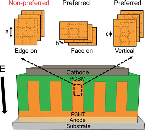
| Schematic of edge-on, face-on and vertical chain orientations of P3HT molecules in a nanoimprinted OPV device of vertically interdigitized and bi-continuous P3HT and PCBM heterojunction. Face-on and vertical orientations are preferred for hole transport due to their short hopping distances b and c, respectively, along the vertical direction of electric field E, compared to the non-preferred edge-on with a large hopping distance a. (Reprinted with permission by The Royal Society of Chemistry) | |
| "In addition to the various nanostructure geometries used for OPV devices, none of the studies in literature investigating NIL induced polymer chain alignment have included solar cell performance results within the same work to directly prove its impact and demonstrate their correlation," Yi Yang, a senior engineer at Globalfoundries and previously a PhD researcher in Hu's and Zakhidov's groups, tells Nanowerk. "To address these issues, we have systematically studied the effects of nanostructure geometry on both chain alignment and device performance. This is the first time to the best of our knowledge that such a study has been carried out." | |
| In their paper, the team demonstrates the effects of nanostructure geometry on the nanoimprint-induced P3HT chain alignment and the performance of nanoimprinted photovoltaic devices. They find that narrower nanostructures with higher aspect ratio are favorable for high performance polymer solar cells. | |
| They observe the dependence of the crystallite orientation on nanostructure geometry such that a larger width of P3HT nanogratings leads to more edge-on chain alignment, which is not favorable for hole transport, while the increase in height gives more vertical alignment, which is favorable for hole transport. | |
| "Consequently, P3HT/PCBM solar cells with the highest density and aspect ratio P3HT nanostructures show the highest power conversion efficiency among others, which is attributed to the efficient charge separation, transport and light absorption," Yang summarizes the findings. | |
| "We believe there is much room to improve our device performance," he continues. "To obtain a better efficiency, one can further increase the aspect ratio of P3HT nanostructures, i.e. decrease the width and increase the height, as predicted by the trend found in this study." | |
| However, a lot of work is still required to realize this practically. | |
| "For example, if we want to further reduce the nanostructure width, e.g. close to the exciton diffusion length (∼10 nm), techniques such as e-beam lithography are needed to prepare the silicon mold," Yang elaborates. "It would be very slow and expensive if we want to prepare molds with a large feature area – at least 1?1 cm2 – to cover several solar cell pixel devices on the same substrate. When it comes to height, we can make silicon molds with deeper trenches at a low cost. However, as shown in our previous study, when a polymer is imprinted, the larger the mold's aspect ratio, the more easily NIL-formed polymer nanostructures can break during de-molding." | |
| Therefore to realize what is predicted in this study, lower cost of mold fabrication and improvement of the de-molding process are needed. | |
| In summary, though, this work helps researchers to better understand the importance of nanostructure geometry on nanoimprinted polymer solar cells and guide them to achieve highly efficient devices using the demonstrated technique. | |
 By
Michael
Berger
– Michael is author of three books by the Royal Society of Chemistry:
Nano-Society: Pushing the Boundaries of Technology,
Nanotechnology: The Future is Tiny, and
Nanoengineering: The Skills and Tools Making Technology Invisible
Copyright ©
Nanowerk LLC
By
Michael
Berger
– Michael is author of three books by the Royal Society of Chemistry:
Nano-Society: Pushing the Boundaries of Technology,
Nanotechnology: The Future is Tiny, and
Nanoengineering: The Skills and Tools Making Technology Invisible
Copyright ©
Nanowerk LLC
|
|
|
Become a Spotlight guest author! Join our large and growing group of guest contributors. Have you just published a scientific paper or have other exciting developments to share with the nanotechnology community? Here is how to publish on nanowerk.com. |
|