| Posted: Oct 21, 2014 | |
Ultra-stretchable silicon for flexible electronics (w/video) |
|
| (Nanowerk Spotlight) The flexibility required when fabricating flexible electronic components has led to the use of plastic substrates, carbon nanomaterials, and different transfer techniques to fabricate flexible devices. One of the biggest obstacles to mass adoption of flexible electronics has been the incompatibility of most of these solutions with industry's state-of-the-art silicon-based CMOS processes – which still produce about 90% of today's electronics. | |
| Researchers have now demonstrated ultra-stretchability in monolithic single-crystal silicon. The design is based on an all silicon-based network of hexagonal islands connected through spiral springs. | |
| "With this structure, we have been able to achieve a remarkable stretch ratio of about 1000% using a brittle material such as silicon," Muhammad Mustafa Hussain, an Associate Professor of Electrical Engineering at King Abdullah University of Science and Technology (KAUST), tells Nanowerk. | |
| Hussain and his team have published their findings in Applied Physics Letters ("Design and characterization of ultra-stretchable monolithic silicon fabric"). | |
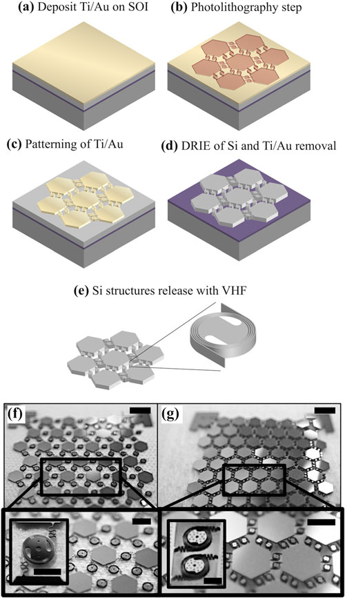
| The fabrication process is based on conventional microfabrication techniques consisting on five basic steps: | |
| Starting with a silicon-on-insulator wafer (50 µm), 1) a gold hard mask is first deposited on silicon-on-insulator and then patterned using 2) photolithography and 3) reactive ion etching (RIE). Next, 4) the silicon is deeply, anisotropically etched (DRIE) until the buried oxide layer is reached and then the hard mask is removed. Finally, 5) the silicon structure is release with vapor hydrofluoric acid, which removes the underlying oxide layer. | |
 |
|
| Summarized fabrication process flow with digital photographs of final designs. (a) Hard mask deposition. (b) Photolithography step. (c) Hard mask’s patterning. (d) Silicon DRIE and hard mask removal. (e) Release of silicon structures with VHF. (f) Digital photographs and zoom-ins of an array of 800 µm-side-hexagons interconnected by single 5 µm-arm spirals (scale bar is 2mm long, 1mm for the first zoom-in and 0.5mm for the spiral zoom-in). (g) Digital photographs and zoom-ins of an array of 800 µm-sidehexagons interconnected by double 2 µm-arm spirals (scale bar is 2mm long, 0.5mm for the first zoom-in and 0.2mm for the spiral zoom-in). (© AIP) | |
| Hussain points out that device implementation can be achieved through CMOS-compatible fabrication previous to the 5-step release process described above. | |
| The resulting single-spiral structures can be stretched to a ratio more than 1000%, while remaining below a 1.2% strain. Moreover, these network structures have demonstrated area expansions as high as 30 folds in arrays. | |
| This video shows the manual stretching of a single 5 µm-arm silicon spiral for 8 cycles, which demonstrates mechanical robustness and reliability. (Video: Integrated Nanotechnology Laboratory, KAUST) | |
| "While handling still remains a challenge, our method can provide ultra-stretchable and adaptable electronic systems for distributed network of high-performance macro-electronics especially useful for wearable electronics and bio-integrated devices," says Hussain. | |
| The researchers are currently working to demonstrate electronic devices implemented on top of their hexagon islands and interconnected through the spiral springs to form stretchable sensor networks with outstanding electrical performance and mechanical robustness. | |
 By
Michael
Berger
– Michael is author of three books by the Royal Society of Chemistry:
Nano-Society: Pushing the Boundaries of Technology,
Nanotechnology: The Future is Tiny, and
Nanoengineering: The Skills and Tools Making Technology Invisible
Copyright ©
Nanowerk LLC
By
Michael
Berger
– Michael is author of three books by the Royal Society of Chemistry:
Nano-Society: Pushing the Boundaries of Technology,
Nanotechnology: The Future is Tiny, and
Nanoengineering: The Skills and Tools Making Technology Invisible
Copyright ©
Nanowerk LLC
|
|
|
Become a Spotlight guest author! Join our large and growing group of guest contributors. Have you just published a scientific paper or have other exciting developments to share with the nanotechnology community? Here is how to publish on nanowerk.com. |
|