| Posted: Jan 14, 2015 | |
Novel mono-elemental semiconductors: arsenene and antimonene join 2D family |
|
| (Nanowerk Spotlight) In the world of 2D materials, single-layer honeycomb crystals like graphene and its elemental analogues – silicene, germanene and stanene – attract much attention due to their exceptional properties. However, the Achilles heel of the electronic structure of graphene, and other elements of the carbon group, is a the zero band gap, which seriously reduces their ability to switch current on and off in transistors, even though with surface functionalization and external electric or strain fields, very small band gaps can be achieved. | |
| Researchers have also fabricated and explored monolayers of typical semiconductors such as MoS2, MoSe2, WS2 and WSe2, as well as few-layered black phosphorus. Such extreme thinning resulted in substantial changes in these materials' electronic structure and hence in new optoelectronic properties and potential device applications. For example, unlike bulk MoS2 with its indirect band gap, monolayer MoS2 was found to be a direct band gap semiconductor and thus displays much stronger luminescence. | |
| They found, however, that the band gaps of most explored 2D systems are below 2.0 eV. | |
| "This situation has greatly impeded the development of 2D semiconductor-based optoelectronic devices with response to the photons with wavelengths less than 620 nm, such as blue and UV light-emitting diodes (LEDs) and photodetectors," Professor Haibo Zeng, Director of the Institute of Optoelectronics & Nanomaterials at Nanjing University of Science and Technology, tells Nanowerk. | |
| In new work, by means of density functional theory computations, Zeng and his group identified novel 2D wide-band-gap semiconductors with high stabilities, namely monolayer arsenene and antimonene. They reported their findings in the January 7, 2015 online edition of Angewandte Chemie International Edition ("Atomically Thin Arsenene and Antimonene: Semimetal–Semiconductor and Indirect–Direct Band-Gap Transitions"). | |
 |
|
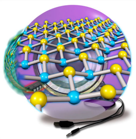
| Illustration of 2D arsenene and antimonene semiconductors as potential applications in devices. (Image: Institute of Optoelectronics & Nanomaterials, Nanjing University of Science and Technology) | |
| Unlike black phosphorus, both arsenic and antimony are typical semimetals in their natural, layered bulk state. However, monolayered arsenene and antimonene are indirect wide-band-gap semiconductors, and under strain, they become direct band-gap semiconductors. | |
| For arsenene and antimonene, such dramatic transitions of electronic properties could open a new door for nanoscale transistors with high on/off ratio, blue/UV optoelectronic devices, and nanomechanical sensors based on new ultrathin semiconductors. | |
| "Interestingly, although both bulk arsenene and antimonene are semimetals, when thinning them into a single atomic layer, our calculations indicate that their electronic structures will be transformed into indirect semiconductors with band gaps of 2.49 and 2.28 eV, respectively," says Shengli Zhang, a researcher at the Institute of Optoelectronics & Nanomaterial and the paper's first author. "Further loading of tiny biaxial strain to these monolayers can transfer them from indirect into direct band-gap semiconductors." | |
| He points out that, currently, there are two very important issues beyond the published results. The first one is the relative position of arsenene and antimonene in the family of 2D crystals, i.e. how are they special and what are their potentials. The second is the experimental reality, i.e. can these 2D materials be fabricated? | |
| "In our lab, we already have fabricated these materials with a thickness of below 10 nm and are now exploring further thinning down to a monolayer," notes Zhang. "We are also exploring the fabrication of transistor devices. Most importantly, though, this work is to induce more researchers to explore these two 2D materials, thus accelerating their development." | |
| After the first experimental demonstration of graphene back in 2004, researchers have mainly focus on 2D materials of the carbon group while ignoring honeycomb sheets of the nitrogen group. Phosphorene, arsenene and antimonene (also including monolayer bismuth with a band gap of 0.99 eV at the HSE06 level of theory) are exciting rediscoveries by the nanomaterials science community and they have quickly become the subject of significant theoretical and experiment investigations. | |
| "We expect that novel 2D mono-elemental semiconductors arsenene and antimonene with wide band gaps can extend the family of semiconductor materials into the nitrogen group," concludes Zeng. | |
 By
Michael
Berger
– Michael is author of three books by the Royal Society of Chemistry:
Nano-Society: Pushing the Boundaries of Technology,
Nanotechnology: The Future is Tiny, and
Nanoengineering: The Skills and Tools Making Technology Invisible
Copyright ©
Nanowerk LLC
By
Michael
Berger
– Michael is author of three books by the Royal Society of Chemistry:
Nano-Society: Pushing the Boundaries of Technology,
Nanotechnology: The Future is Tiny, and
Nanoengineering: The Skills and Tools Making Technology Invisible
Copyright ©
Nanowerk LLC
|
|
|
Become a Spotlight guest author! Join our large and growing group of guest contributors. Have you just published a scientific paper or have other exciting developments to share with the nanotechnology community? Here is how to publish on nanowerk.com. |
|