Nanotechnology News – Latest Headlines
Voyage of the DNA treader
At January's TEDxCaltech conference, researchers will present a one-molecule robot capable of following a trail of chemical breadcrumbs.
December 30, 2010 Read more
NCKU distinguished Prof. Kwang-Lung Lin selected 2011 IEEE Fellow and 2010 MRS-T Fellow
Distinguished Prof. Kwang-Lung Lin of the Department of Materials Science and Engineering at National Cheng Kung University (NCKU), Tainan, Taiwan, the Deputy Executive Director of Industrial Technology Research Institute (ITRI) South, has received the honorary title of 2011 Institute of Electrical and Electronics Engineers (IEEE) Fellow with his outstanding achievement on the research of lead-free solder alloy and its material response, and also won the title of 2010 Materials Research Society Taiwan (MRS-T) Fellow.
December 29, 2010 Read more
Researchers overcome fundamental obstacle in developing breathalyzers for medical diagnostics
Researchers have overcome a fundamental obstacle in developing breath-analysis technology to rapidly diagnose patients by detecting chemical compounds called 'biomarkers' in a person's respiration in real time.
December 28, 2010 Read more
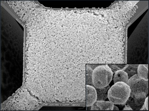
Singapore consortium learns from nature to produce new chemical-free, anti-bacteria plastic 'skins'
Five new US, European and Japanese companies join A*STAR's Industrial Consortium On Nanoimprint to engineer marine life-inspired anti-microbial surfaces for use on ships, lenses and medical devices.
December 28, 2010 Read more
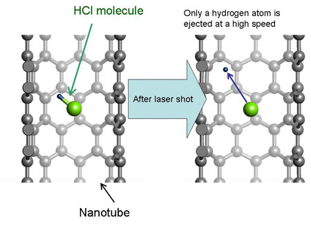
'Earth Simulator' succeeds in the world's first simulation-based prediction of photochemical reactions inside carbon nanotubes
NEC Corporation announced that it succeeded in the world's first simulation-based prediction of laser-induced photochemical reactions that can efficiently eject a hydrogen atom from a hydrogen chloride molecule trapped inside a carbon nanotube.
December 28, 2010 Read more
NIOSH requests information on occupational exposure to carbon nanotubes and nanofibers
The National Institute for Occupational Safety and Health (NIOSH) requests comments on the draft Current Intelligence Bulletin Occupational Exposure to Carbon Nanotubes and Nanofibers, NIOSH Docket Number: NIOSH 161-A.
December 27, 2010 Read more
California chemical information call-in: Nanometals, nanometal oxides, and quantum dots
Pursuant to Health and Safety Code section 57019(d), the Department of Toxic Substances Control (DTSC) formally announces this request for information regarding analytical test methods, and other relevant information, from manufacturers of the following nanomaterials: Nano Silver, Nano Zero Valent Iron, Nano Titanium Dioxide, Nano Zinc Oxide, Nano Cerium Oxide, Quantum Dots.
December 27, 2010 Read more
Canyons im Nanokosmos - die Struktur weicher Materialien vermessen
Chemnitzer Physiker stellen neue zerstoerungsfreie Messmethode fuer die Oberflaechenstruktur weicher Materialien vor.
December 27, 2010 Read more
Researchers fabricate first single crystal diamond nanoelectromechanical switch
Researchers succeeded in the batch fabrication of suspended structures (cantilevers and bridges) of single crystal diamond for nano/micro electromechanical system (NEMS/MEMS). Based on this process, they achieved in the world the first single crystal diamond NEMS switch.
December 24, 2010 Read more
A comparative methodology for estimating the economic value of innovation in nanotechnologies
Defra, the UK Department of Environment, Food and Rural Affairs, has published a five piece set of reports (free downloads) that describe a methodology for performing a comparative valuation of a nanotechnology against an incumbent technology.
December 24, 2010 Read more
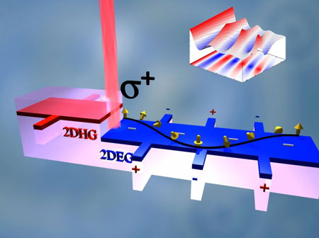
Breakthrough gives a new spin to semiconductor nanoelectronics
An international team of researchers has announced a breakthrough that gives a new spin to semiconductor nanoelectronics and the world of information technology. The team has developed an electrically controllable device whose functionality is based on an electron's spin.
December 23, 2010 Read more
Scientific discovery moves racetrack memory closer
IBM Researchers today revealed a previously unknown aspect of key physics inside Racetrack memory -- a new technology design which stands to improve memory capabilities within mobile phones, laptop computers and business-class servers. This new class of memory could enable devices to store much more information - as much as a factor of 100 times greater - while using much less energy than today's designs.
December 23, 2010 Read more
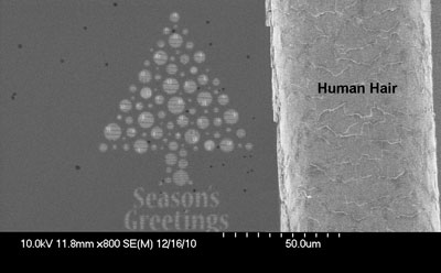
Engineers produce the world's smallest Christmas card
It wouldn't look good on the mantelpiece and is bound to get lost in the post - it's the world's smallest Christmas card. Invisible to the naked eye, the card is so small that 8276 of them could fit on an area the size of a first class stamp.
December 23, 2010 Read more
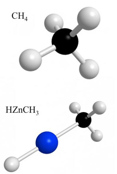
Milestone: A methane-metal marriage
For the first time, chemists have succeeded in plugging a metal atom into a methane gas molecule, thereby creating a new compound that could be a key in opening up new production processes for the chemical industry, especially for the synthesis of organic compounds, which in turn might have implications for drug development.
December 23, 2010 Read more
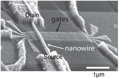
Better control of building blocks for quantum computer
Scientists from the Kavli Institute of Nanoscience at Delft University of Technology and Eindhoven University of Technology in The Netherlands have succeeded in controlling the building blocks of a future super-fast quantum computer. They are now able to manipulate these building blocks (qubits) with electrical rather than magnetic fields, as has been the common practice up till now.
December 23, 2010 Read more
 Subscribe to our Nanotechnology News feed