Nanotechnology Spotlight – Latest Articles
 Subscribe to our Nanotechnology Spotlight feed
Showing Spotlights 2313 - 2320 of 3575 in category All (newest first):
10 years of nanotechnology risk research - a European status update
A group of experts from the chemical industry and various research laboratories in Germany have published a report on the current status of risk research on nanotechnology materials and applications. The report - 10 Years of Research: Risk Assessment, Human and Environmental Toxicology of Nanomaterials - provides an overview of the current state of risk assessment and toxicological research into nanomaterials. It also lists and summarizes the national and European projects on toxicology on various nanomaterials. In their report, the working group "Responsible Production and Use of Nanomaterials" has drawn up a list of topics and priorities which need to be addressed; activities and projects which have already been carried out; are currently on-going; or are still at the planning stage. The main focus of our considerations is on Germany, with a wider outlook on papers and results at European level.
February 28, 2012
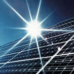
Practical roadmap and efficiency limits to nanotechnology photovoltaics
The significant research interest in the engineering of photovoltaic (PV) structures at the nanoscale is directed toward enabling reductions in PV module fabrication and installation costs as well as improving cell power conversion efficiency. With the emergence of a multitude of nanostructured photovoltaic device architectures, the question has arisen of where both the practical and the fundamental limits of performance reside in these new systems. A particular advantage of nanostructured materials is the tunability of their optical and electronic properties, which enables improved PV power conversion efficiencies by implementing strategies for reducing thermal losses. A recent review article addresses the limits to the performance of molecular, organic, polymeric, dye-sensitized, and colloidal quantum dot-based solar cells.
February 23, 2012
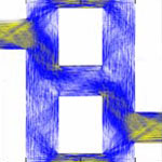
Traffic planning in the quantum world
Researchers have demonstrated that electrons in nanoscale networks can behave like car drivers in congested cities. Traffic planners are sometimes faced with a rather counter-intuitive observation - adding a new road to a congested road network can lead to a deterioration of the overall traffic situation, i.e. longer trip times for individual road users. Or, in reverse, blocking certain streets in a complex road network can counter-intuitively reduce congestion. This has become known as the Braess paradox. Researchers have now applied the concept of the Braess paradox to the quantum world. By combining quantum simulations of a model system and scanning-probe experiments, they have shown that an analogue of the Braess paradox can occur in mesoscopic semiconductor networks, where electron transport is governed by quantum mechanics. The paradox manifests itself by an increase of the conductance network when one arm in the network is partially blocked in a controlled manner.
February 21, 2012
Diamond gives graphene devices a major performance boost
Graphene is an excellent conductor of heat and might be an ideal material for thermal management in nanoelectronics. In field-effect transistors or interconnects most of the heat propagates directly below the graphene channel in the direction of the heat sink, that is, the bottom of a silicon wafer. For this reason, the highly thermally resistive silicon layers act as a thermal bottleneck, preventing the full utilization of graphene's excellent intrinsic properties. The breakdown current density in typical graphene devices is a hundred times larger than the fundamental limit in metals, which is set by electromigration. Researchers wanted to see if we can push the breakdown current density in graphene even further by better removal of dissipated heat. They managed to do it with the help of high-quality synthetic diamond. The graphene transistors or interconnects on synthetic diamond can sustain current densities which are a thousand times larger than in metals.
February 20, 2012

Speeding up the fabrication of metal-organic framework devices
Metal-organic frameworks (MOFs) are well-ordered, lattice-like crystals. The nodes of the lattices are metals which are connected by organic molecules. Their controlled nanometer-sized pores provide MOFs with the potential to be used in next generation gas storage, gas separation and sensors. With their special structure and large surface area, MOFs open up new opportunities for alternative systems for gas and energy storage (e.g. carbon dioxide and hydrogen storage), in catalysis, chemical sensing, as nanoreactors, and in drug delivery, making them hugely interesting for both university research and industry. Researchers have now achieved the first microfluidic method for patterning MOF crystals. As such, high-throughput single crystal patterning is achieved with an unprecedented degree of flexibility.
February 16, 2012

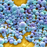
New study shows that titanium dioxide nanoparticles are ubiquitous in food products
Following up on our recent Nanowerk Spotlight on nanofoods, new research shows that consumers could be exposed to nanoparticles in food by a much larger degree than has been expected so far. For a modern consumer it is hard to avoid titanium dioxide (TiO2) - a widely used additive in food, personal care and other household products. Approximately 7 million tons of bulk TiO2 are produced annually and used as white pigment in order to provide whiteness and opacity to foods and other products. Many applications of titanium dioxide would benefit from smaller primary particle sizes, and we can expect the percentage of TiO2 that is produced in or near the nano range to increase.
February 15, 2012
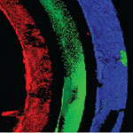
Tissue engineering of 3D tubular structures
At the core of tissue engineering is the construction of three-dimensional scaffolds out of biomaterials to provide mechanical support and guide cell growth into new tissues or organs. In another advance for the field, researchers have now demonstrated a strategy to fabricate tubular structures with multiple types of cells as different layers of the tube walls. This method may be widely used in simulation of many tubular tissues and enriches the toolbox for 3D micro/nanofabrication by initially patterning in 2D and transforming it into 3D. Tubular tissues such as the trachea, blood vessels, lymph vessels, and intestines, have two distinguishing features: They have specific 3D shapes;and they have different types of cells at specific locations, i.e. different parts of the tube wall are made up of different cells. Mimicking both of these features is a prerequisite for fabricating functional tubular tissues in vitro, and the realization of structural-tissue mimicry may have wide applications.
February 14, 2012
Exploding microcapsules track down and kill cancer cells
With the advent of nanomedicine, the concept of a "magic bullet" to fight cancer is getting closer to reality. Previously an idea straight out of science fiction, researchers around the world are working on perfecting nano- and microscale drug carriers that get injected into the body, transport themselves to the correct target, such as a tumor, and deliver the required dose of a medication or other substance to effectively destroy or repair this target. The controlled drug release required by these systems, however, has proven to be quite a challenging issue. To avoid the side effects of prematurely released toxic cancer drugs on healthy tissues, researchers have designed and fabricated an "active defense" system which could effectively keep the drug entrapped in its carrier in the blood and normal tissues whereas it would allow the explosive drug release under the right physiopathological stimuli once the drug carrier reaches the cancerous tissues.
February 13, 2012