| Posted: Feb 16, 2012 |
Speeding up the fabrication of metal-organic framework devices |
| (Nanowerk Spotlight) Metal-organic frameworks (MOFs) are well-ordered, lattice-like crystals. The nodes of the lattices are metals – such as copper, zinc, nickel or cobalt – which are connected by organic molecules. Their controlled nanometer-sized pores provide MOFs with the potential to be used in next generation gas storage, gas separation and sensors. |
| With their special structure and large surface area, MOFs open up new opportunities for alternative systems for gas and energy storage (e.g. carbon dioxide and hydrogen storage), in catalysis, chemical sensing, as nanoreactors, and in drug delivery, making them hugely interesting for both university research and industry (chemical giant BASF already started industrial-scale synthesis of MOFs in 2010). |
| "Exploitation of the unique properties of these materials requires the successful integration and immobilization of MOF crystals in functional devices, but this has proven to be very challenging," Daan Witters, a PhD student in Jeroen Lammertyn's MeBioS biosensor group at KU Leuven in Belgium, tells Nanowerk. "Depending on the intended application, one wants to deposit MOF crystals as thin crystalline films, or as single crystals. Our goal was to develop a novel miniaturized and highly automated method for the high-throughput generation of arrays of single MOF crystals on a planar surface, while achieving high monodispersity and spatially resolved control over the coating area of interest." |
| As the group reports in the February 2, 2012 online edition of Advanced Materials ("Digital Microfluidic High-Throughput Printing of Single Metal-Organic Framework Crystals"), they achieved the first microfluidic method for patterning MOF crystals. As such, high-throughput single crystal patterning is achieved with an unprecedented degree of flexibility. |
| "Our technology combines microfluidic high-throughput printing of single MOF crystals with a high degree of flexibility, and does not rely on any expensive equipment," says Witters, who is first author of the paper. "This can enhance the integration of MOF materials in functional devices, and strengthen their applicability in future sensing, separation, and storage applications. Moreover, it provides a useful tool for the studying of MOF materials at the single-crystallite level." |
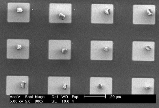 |
| SEM image of an array of single HKUST-1 crystals that were printed in hydrophilic micropatches of 20 µm x 20 µm on a digital microfluidic chip. (Image: Daan Witters, KU Leuven) |
| By using digital microfluidic technology, the new device transports individual micro- to nanometer sized droplets on hydrophobic surfaces by applying a sequence of electrical signals to embedded electrode arrays. This allows droplets to be actuated on a pattern of actuation electrodes with a very high degree of flexibility. |
| "By creating hydrophilic-in-hydrophobic micropatterns on the chip surface, and transporting droplets over these patterns, femtoliter-sized droplets are deposited inside the hydrophilic micropatches due to their selective wettability," explains Witters. "As such, we demonstrate the printing of up to 6400 femtoliter droplets per second. When applying this technology to the printing of droplets of MOF synthesis solutions containing inorganic and organic building blocks, huge arrays of single MOF crystals are deposited inside the hydrophilic micropatches." |
| He points out that this deposition speed demonstrates the high-throughput capability of the new deposition technology, especially when comparing it to drop-by-drop, hence crystal-by-crystal, printing methods such as dip-pen lithography. |
| Moreover, the single crystals show excellent monodispersity while their size can be tuned by tailoring the size of the hydrophilic micropatches. |
| To demonstrate the capabilities of the new system, the researchers applied this technology to the patterning of HKUST-1 (Cu3(BTC)2) crystals, a much studied MOF material. |
| "In future work, we anticipate that this high-throughput technology can easily enable post-synthesis modification of printed MOF crystals with different functionalities, or perform sequential functionalization of MOF crystals by fabricating heterostructured core-shell architectures, among others" says Witters. |
 By
Michael
Berger
– Michael is author of four books by the Royal Society of Chemistry:
Nano-Society: Pushing the Boundaries of Technology (2009),
Nanotechnology: The Future is Tiny (2016),
Nanoengineering: The Skills and Tools Making Technology Invisible (2019), and
Waste not! How Nanotechnologies Can Increase Efficiencies Throughout Society (2025)
Copyright ©
Nanowerk LLC
By
Michael
Berger
– Michael is author of four books by the Royal Society of Chemistry:
Nano-Society: Pushing the Boundaries of Technology (2009),
Nanotechnology: The Future is Tiny (2016),
Nanoengineering: The Skills and Tools Making Technology Invisible (2019), and
Waste not! How Nanotechnologies Can Increase Efficiencies Throughout Society (2025)
Copyright ©
Nanowerk LLC
|

Become a Spotlight guest author! Join our large and growing group of guest contributors. Have you just published a scientific paper or have other exciting developments to share with the nanotechnology community? Here is how to publish on nanowerk.com. |
