Showing Spotlights 297 - 304 of 338 in category All (newest first):
 Carbon nanotubes (CNTs) have not yet met commercial expectations from a decade ago, and now hot on its heels is graphene. Graphene is considered a hot candidate for applications such as computers, displays, photovoltaics, and flexible electronics. The biggest opportunity for both materials is in printed and potentially printed electronics. In a comparably short time a large amount of graphene materials have become commercially available contributing to further advancements and application development. At a fraction of the weight and cost of CNTs, graphene may displace carbon nanotubes and even indium tin oxide in some applications. Flexible, see-through displays may be the one application that finally puts graphene into the commercial spotlight.
Sep 28th, 2011
 Electronic memory devices are increasingly expected to provide not only greater storage density, but also faster access to information. As storage density increases, however, power consumption and unwanted heat generation also increase, and the fidelity of accessing the memory is frequently diminished. Various platforms exist to overcome these hurdles and, increasingly, graphene finds it way into computer memory technology. The most recent example are experiments that demonstrate the benefits of graphene as a platform for flash memory which show the potential to exceed the performance of current flash memory technology by utilizing the intrinsic properties of graphene.
Sep 5th, 2011
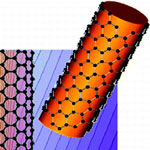
 Surface energy is ubiquitous in nature and it plays an important role in many scientific areas such as for instance surface physics, biophysics, surface chemistry, or catalysis. Prior to the area of nanotechnology it has been impractical to consider utilizing surface energy as an energy source because there are few molecules or atoms involved in the surface interaction and the density of surface energy is low. Now, however, due to the lower power consumption requirements of nanoscale devices and the higher specific surface area for nanomaterials it appears attractive to use surface energy at the nanoscale. In new work, researchers have investigated how the flow of water over surfaces coated with graphene could generate small amounts of electricity.
Jul 25th, 2011
 The field of single-molecule magnets is very promising, since an individual magnetic molecule represent the ultimate size limit to store and processing information. Magnetic molecules are considered very promising for spintronics since they can store a bit of information in an extremely small volume. However, in order to make magnetic molecules work, one has to find a way to measure their magnetization. Usual approaches are often very invasive and may lead to a strong perturbation of the properties of the molecules. A European research team has now designed and realized a novel hybrid spintronic nanodevice where the state of the molecule is measured 'indirectly', through a sensor coupled with the molecule.
Jul 5th, 2011
 There has been tremendous interest in cloaking technology using metamaterials and there are two exciting possibilities to obtain drastic scattering reduction from moderately-sized objects. One is the concept of plasmonic cloaking, which is based on the use of a thin metamaterial cover to suppress the scattering from a passive object. The second one is the concept of mantle cloaking, which is based on a simple impedance surface to achieve similar effects. Now, new research shows that even a single layer of atoms, with the exciting conductivity properties of graphene, may achieve similar functionality in planar and cylindrical geometries. Once realized, this concept represents the 'thinnest' possible cloak, operating in the THz spectrum.
Jun 30th, 2011
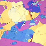
 Graphene has two distinct types of edges produced when it is cut - armchair type or zigzag type - which correspond to the two crystal axis of graphene. These edge types have distinct electronic, magnetic, and chemical properties, and being able to pattern graphene along particular crystallographic directions to leave edges consisting of a single chirality is crucial for the fabrication of graphene nanoribbon and nanoelectronics devices. A widely discussed method for the patterning of graphene is the channelling of graphite by metal nanoparticles in oxidizing or reducing environments. Researchers now report the live nanoscale observation of this channelling process by silver nanoparticles.
Jun 13th, 2011
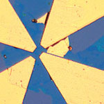
 Unlike silicon, graphene lacks an electronic band gap - the gap being an energy range that cannot be occupied by electrons - and therefore has no switching capability; which is essential for electronics applications. Opening an energy gap in graphene's electron energy spectrum is therefore a critical prerequisite for instance for creating graphene transistors. That's where strain engineering of graphene comes in. Researchers have discovered that local strain in a graphene sheet can alter its conducting properties. By varying the amount of local strain, transport gaps can be tailored. In new work, researchers present a new and novel mechanism for gap opening in strained graphene via electrostatic gates and show that it can be important also in realistic situations.
Jun 8th, 2011
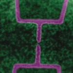
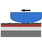 Interaction forces between contact surfaces, such as the adhesion and friction forces, are crucial in many applications at the nanoscale because of the high surface-to-volume ratio of nanomaterials and nanodevices. Over the last decade, various solid lubricant materials, micro/nano patterns, and surface treatment processes have been developed for efficient operation and extended lifetime in MEMS/NEMS applications, and for various fabrication processes such as nanoimprint lithography and transfer printing. From a practical viewpoint, large-area CVD-graphene holds the greatest promise as a solid lubricant because of its excellent scalability and transferability. So far, the tribological characteristics of CVD-graphene at the micro- and nanoscale have not been reported yet. Researchers have now demonstrated the feasibility of using large-area CVD-graphene as a solid lubricant.
May 25th, 2011
 Subscribe to our Nanotechnology Spotlight feed