Showing Spotlights 33 - 40 of 43 in category All (newest first):
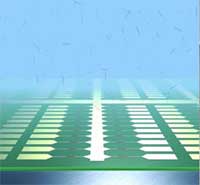
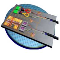 In its everlasting quest to deliver more data faster and on smaller components, the silicon industry is moving full steam ahead towards its final frontiers of size, device integration and complexity. We have covered this issue numerous times in previous Spotlights. As the physical limitations of metallic interconnects begin to threaten the semiconductor industry's future, one group of researchers and companies is betting heavily on advances in photonics that will lead to combining existing silicon infrastructure with optical communications technology, and a merger of electronics and photonics into one integrated dual-functional device. Today, silicon underpins nearly all microelectronics but the end of the road for this technology has clearly come into view. Photonics is the technology of signal processing, transmission and detection where the signal is carried by photons (light) and it is already heavily used in photonic devices such as lasers, waveguides or optical fibers. Optical technology has always suffered from its reputation for being an expensive solution, due to its use of exotic materials and expensive manufacturing processes. This prompted research into using more common materials, such as silicon, for the fabrication of photonic components, hence the name silicon photonics. Although fiber-optic communication is a well-established technology for information transmission, the challenge for silicon photonics is to manufacture low-cost information processing components. Rather than building an entirely new industrial infrastructure from scratch, the goal here is to to develop silicon photonic devices manufactured using standard CMOS techniques. A recent review paper takes a look at the state of silicon photonics and identifies the challenges that remain on the path to commercialization.
Mar 14th, 2008
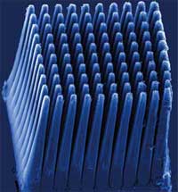
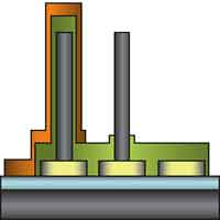 A memory chip is an integrated circuit made of millions of transistors and capacitors. In the most common form of computer memory, dynamic random access memory (DRAM), a transistor and a capacitor are paired to create one memory cell, which represents a single bit of data. The capacitor holds the bit of information, either a 0 or a 1. The transistor acts as a switch that lets the control circuitry on the memory chip read the capacitor or change its state. Because each bit stored in a chip is controlled by one transistor, memory capacities tend to expand at the same pace as the number of transistors per chip - which still follows Moore's Law and therefore currently doubles every 18 months. The problem is that the capacitor - consisting of two charged layers separated by an insulator - can shrink only so far. The thinner insulators get the more they allow charges to tunnel through. Tunneling increases the leakage current, and therefore the standby power consumption. Eventually the insulator will break down. Researchers have been trying to develop electromechanically driven switches that can be made small enough to be an alternative to transistor-switched silicon-based memory. Electromechanical devices are suitable for memory applications because of their excellent ON-OFF ratios and fast switching characteristics. With a mechanical switch there is physical separation of the switch from the capacitor. This makes the data leakage problem much less severe. Unfortunately they involve larger cells and more complex fabrication processes than silicon-based arrangements and therefore have not been so far an alternative to scaling down beyond semiconductor transistors. Researchers now have reported a novel nanoelectromechanical (NEM) switched capacitor structure based on vertically aligned multiwalled carbon nanotubes (CNTs) in which the mechanical movement of a nanotube relative to a carbon nanotube based capacitor defines ON and OFF states.
Jan 10th, 2008
 Continuing miniaturization has moved the semiconductor industry into the nano realm with leading chip manufacturers well on their way to CPUs using 32nm process technology (expected by 2009). There are some real challenges ahead for chip designers, particularly in moving deeper and deeper into the nanoscale, where at some point in the near future they will reach physical limits of the traditional logic MOSFET (metal-oxide-semiconductor field-effect transistor) structure. In addition to physical barriers, semiconductor companies will also reach economic barriers where profitability will be squeezed hard in view of the exorbitant costs of building the necessary manufacturing capabilities if present day technologies are extrapolated. Quantum and coherence effects, high electric fields creating avalanche dielectric breakdowns, heat dissipation problems in closely packed structures and the relevance of single atom defects are all roadblocks along the current road of miniaturization. Enter nanoelectronics (note that microelectronics, even if the gate size of the transistor is below 100 nm, is not an implementation of nanoelectronics, as no new qualitative physical property related to reduction in size are being exploited). Its goal is to process, transmit and store information by taking advantage of properties of matter that are distinctly different from macroscopic properties. Understanding nanoscale transport and being able to model and simulate nanodevices requires an entirely new generation of simulation tools and techniques.
Jul 3rd, 2007
 Better magnetic storage devices for computers and other electronics could result from new work by researchers in Germany and the United States.
May 28th, 2007
 The semiconductor industry is on its way to 32 nm processor technology, expected to be commercialized around 2009, and the day might be near when transistors will reach the limits of miniaturization at atomic levels and put an end to the currently used fabrication technologies. Apart from the issues of interconnect density and heat dissipation, which some researchers hope to address with carbon nanotube-based applications, there is the fundamental issue of quantum mechanics that will kick in once chip design gets down to around 4 nm. This is where semiconductor dimensions have become so small that quantum effects would dominate the circuit behavior. Computer designers usually regard this as a bad thing because it might allow electrons to leak to places where they are not wanted. In particular, the tunneling of electrons and holes - so-called quantum tunneling - will become too great for the transistor to perform reliable operations. The result would be that the two states of the switch could become indistinguishable. Quantum effects can, however, also be beneficial. A group of researchers has now shown that a single bit of data might be stored on, and again retrieved from, a single atom. Just don't expect this in your computer anytime soon, though.
May 24th, 2007
 Over the next few years, semiconductor fabrication will move from the current state-of-the-art generation of 90 nanometer processes to the next 65 nm and 45 nm generations. Intel is even already working on 32 nm processor technology, code-named "Westmere", that is expected to hit the market sometime around 2009. The result of these efforts will be billion-transistor processors where a billion or more transistor-based circuits are integrated into a single chip. One of the increasingly difficult problems that chip designers are facing is that the high density of components packed on a chip makes interconnections increasingly difficult. In order to be able to continue the trend predicted by Moore's law, at least for a few more years, researchers are now turning to alternative materials for transistors and interconnect and one of the prime candidates for this job are single-walled carbon nanotubes (SWCNT). However, one of the biggest limitations of conventional carbon nanotube device fabrication techniques today is the inability to scale up the processes to fabricate a large number of devices on a single chip. Researchers in Germany have now demonstrated the directed and precise assembly of single-nanotube devices with an integration density of several million devices per square centimeter, using a novel aspect of nanotube dielectrophoresis. This development is a big step towards commercial realization of CNT-based electronic devices and their integration into the existing silicon-based processor technologies.
May 16th, 2007
 For computer chips, 'smaller and faster' just isn't good enough anymore. Power and heat have become the biggest issues for chip manufacturers and companies integrating these chips in everyday devices such as cell phones and laptops. The computing power of today's computer chips is provided mostly by operations switching at ever higher frequency. This physically induced power dissipation represents the limiting factor to a further increase of the capability of integrated circuits. Heat dissipation of the latest Intel processors has become a widely discussed issue. By the end of the decade, you might as well be feeling a rocket nozzle than touching a chip. And soon after 2010, computer chips could feel like the bubbly hot surface of the sun itself. As the electronics industry continues to churn out smaller and slimmer portable devices, manufacturers have been challenged to find new ways to combat the persistent problem of thermal management. New research suggests that the integration of carbon nanotubes (CNTs) as heat sinks into electronic devices might provide a solution to this problem.
Apr 12th, 2007
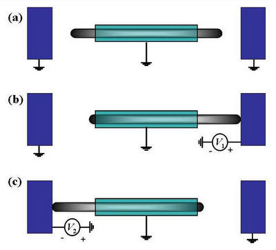 Non-volatile random access memory (NVRAM) is the general name used to describe any type of random access memory which does not lose its information when power is turned off. This is in contrast to the most common forms of random access memory today, DRAM and SRAM, which both require continual power in order to maintain their data. NVRAM is a subgroup of the more general class of non-volatile memory types, the difference being that NVRAM devices offer random access, as opposed to sequential access like hard disks. The best-known form of NVRAM memory today is flash memory, which is found in a wide variety of consumer electronics, including memory cards, digital music players, digital cameras and cell phones. One problem with flash memory is its relatively low speed. Also, as chip designers and engineers reach size barriers in downscaling the size of such chips, the research focus shifts towards new types of nanomemory. Molecular-scale memory promises to be low-power and high frequency: imagine a computer that boots up immediately on powering up and that writes data directly onto its hard drive making saving a thing of the past. Researchers are designing the building blocks for this type of memory device using telescoping carbon nanotubes as high-speed, low power microswitches. The design would allow the use of these binary or three-stage switches to become part of molecular-scale computers.
Feb 14th, 2007
 Subscribe to our Nanotechnology Spotlight feed