Showing Spotlights 481 - 488 of 625 in category All (newest first):
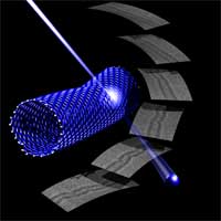 Electron microscopy is a delicate balancing act between using the highest energy electrons possible in order to obtain the best image while avoiding destruction of the sample under investigation. Trouble is, the electron beam does not just observe, it also interacts with the structure that is observed. This can be critical for fragile samples such as nanostructures: the transfer of energy from the electron beam can be sufficient that atoms are knocked right out of the material. In the worst case the sample is destroyed in front of your eyes. Scientists in Orsay, France have turned this problem to their advantage. They have developed a new approach to shaping nanomaterials atom by atom, using a scanning transmission electron microscope (STEM) as a nanometrically precise cutting tool. In this way they 'carve' their materials, such as carbon nanotubes, by removing individual atoms from specifically chosen locations. This technique has the added advantage that scientists can observe what they are doing at the same time. The new technique demonstrates a 'nanoelectron- lithography' of single walled nanotubes, a top down approach to locally control their nanostructures.
Feb 8th, 2008
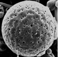
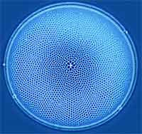 Diatoms are a major group of hard-shelled algae and one of the most common types of phytoplankton. A characteristic feature of diatom cells is that they are encased within a unique cell wall made of silica. Silicate materials are very important in nature and they are closely related to the evolution of living organisms. Diatom walls show a wide diversity in form, some quite beautiful and ornate, but usually consist of two symmetrical sides with a split between them, hence the group name. There is great potential for the use of diatoms in nanotechnology. This potential lies in the pores and channels which give rise to a greatly increased surface area, and the silica structure which lends itself to chemical modification. In addition there is a huge variety in the sizes and shapes of diatoms available, providing scope for the selection of a particular species of diatom tailored to a particular requirement. Researchers in the UK have demonstrated that the silica walls of diatoms can be used for the attachment of active biomolecules, such as antibodies, using either primary amine groups or the carbohydrate moiety. These modified structures can, therefore, be used for antibody arrays or for use in techniques such as immunoprecipitation.
Feb 7th, 2008
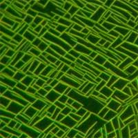 The vision of revolutionary bottom-up nanotechnology is based on a concept of molecular assembly technologies where nanoscale materials and structures self-assemble to microscale structures and finally to macroscopic devices and products. We are a long way from realizing this vision but researchers are busily laying the foundation for nanoscale engineering. Assembling nanoscopic components into macroscopic materials is an appealing goal but one of the enormous difficulties lies in bridging approximately six orders of magnitude that separate the nanoscale from the macroscopic world. Until machinery capable of automated and industrial-scale nano-assembly can be built, the parallelism of chemical synthesis and self-assembly is necessary when controlling materials at the nanoscale. An obvious direct approach to molecular nanotechnology therefore is to start with organic molecules as building blocks. Modest from the viewpoint of molecular manufacturing visionaries, but quite fascinating to a lot of scientists, research into nanofibers, as a modification of organic crystals, is making good progress. New research results coming out of Denmark offer the basis for a novel organic-molecule-based nanotechnological concept that allows for a multitude of applications in fundamental research and in device applications. Essentially, this concept is based on three steps: 1) directed self-assembled surface growth of nanofibers from functionalized molecules; 2) transfer and manipulation of individual fibers as well as of ordered arrays; and 3) device integration.
Feb 1st, 2008
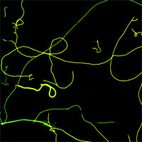 'Smart' is the key buzz word used by materials engineers when they describe the future of coatings, textiles, building structures, vehicles and just any material that you can think of. Materials are made 'smart' when they are engineered to have properties that change in a controlled manner under the influence of external stimuli such as mechanical stress, temperature, humidity, electric charge, magnetic fields etc. Nature of course is full with 'smart' materials that are capable of adapting to new tasks, are self-healing, and can self-assemble autonomously simply out of a solution of building blocks. Duplicating this feat with man-made materials will one day become a reality thanks to nanotechnology. Scientists not only dream about self-repairing cars or building walls that turn transparent like windows, they are actively working on the first steps towards these goals. Simple smart materials (that are not nanotechnology based) are already a reality, such as piezoelectric materials and shape memory alloys. Emerging nanotechnologies are now about to give scientists the tools to take smart materials to the next performance level. For instance, the European project Inteltex is developing a new, multifunctional textile that could be used as a wallpaper to detect temperature changes or chemical leakage or that could be used in medical and protective wear to monitor body temperature and mechanical stress. MIT's Institute for Soldier Nanotechnologies works on smart surfaces that switch properties. Nanotechnology-enabled smart materials are still very early days but basic progress is being made. Another small building block towards smart materials was recently reported by Italian researchers who demonstrated photo-switchable nanofibers based on the reversible transformation between two molecular photochemical states, exhibiting different chemico-physical characteristics.
Jan 31st, 2008
 Hollow polymeric micro- and nanoparticles have numerous existing and many anticipated applications in drug delivery, ranging from the controlled release of drugs, cosmetics, inks, pigments or chemical reagents to the protection of biologically active species, and removal of pollutants. Encapsulation also allows drug targeting via cell and tissue-specific ligands. There is a variety of methods available for synthesis of polymer microspheres with hollow interiors. The hollow particles are most commonly prepared by coating the surfaces of colloidal templates with thin layers of the desired material (or its precursor), followed by selective removal of the templates by means of calcination or chemical etching. For polymers, methods such as emulsion polymerization, phase separation, cross-linking of micelles and self-assembly have also been demonstrated for generating hollow structures. The hollow polymer particles produced by these methods present either a closed-core-shell structure or many small pores on their surface. However, these synthetic approaches present limitations on the choice of polymers that can be produced as hollow microspheres. Also, the number, size and shape of the surface pores can not be easily manipulated. When these materials are used for encapsulation-related applications, the encapsulation of the desired functional materials is usually too slow and/or too labor-intense. These problems have motivated scientists to develop the synthesis of a new class of polymer microspheres, which they called microscale fish bowls. Their unique feature consists in the presence of one big pore on their surface that allows easy and fast diffusion of a functional material to be encapsulated. Another new feature is that this newly developed method presents no limitations on the choice of polymers that can be produced as microscale fish bowls.
Jan 25th, 2008
 Sophisticated optical lithography techniques have been developed by the semiconductor industry to pack more and more transistors onto chips. On the road to a billion transistors per chip, Intel has already developed transistors so small that 200 million of them could fit on the head of a pin. As if that wasn't small enough, scientists are pushing further down, hoping to be able one day to reliably (and affordably) control surface features as small as 1 nm. With today's technology, cost-effective fabrication in the sub-50 nm range is a major challenge. Given the advanced development of (nano)lithography it is not surprising that various forms of it are the most common techniques used by nanotechnology researchers for manipulating sub-100 nm surface features. With the current state of optical lithography it appears that traditional commercial lithography techniques will not be cost effective below 30 nm. State-of-the-art electron beam lithography (EBL) has been proved to be capable of delivering resolution in the 10 nm range. Unfortunately, EBL is slow, very expensive and it is very unlikely that it can effectively go below 10 nm. The same limitations hold for x-rays and focused ion beams (FIBs), with additional tremendous difficulties in developing equipment for beam manipulation and focusing on nanometer scales.
Jan 24th, 2008
 Nature has excelled in designing molecular motors, something nanotechnology researchers are still having a hard time with. The potential for nano-actuators (a nanoscale device that creates automatic motion by converting various forms of energy to rotary or linear mechanical energy) is huge - basically any active system that performs some kind of work requires an energy source. Applications reach from simple pumps on lab-on-a-chip devices to move nanoliters of fluid around to nanoscale motors for nanorobotic systems. One of the challenges of designing such a motor for the nano realm is that during the design of a nano-actuator the tradeoffs among range of motion, force, speed (actuation frequency), power consumption, control accuracy, system reliability, robustness, load capacity, etc. must be taken into consideration. Most microscale systems are currently achieved by relatively large external actuators such as syringe pumps, or high voltage power supplies, which negates the advantages of the microfabricated systems. That's why scientists are quite intrigued by the opportunity to use biological organisms to construct mechanical actuators in engineered systems at the micro- or even nanoscale. An extremely powerful biological motor is the bacterial flagellar motor found in organisms such as Escherichia coli or Serratia marcescens. Bacteria draw chemical energy directly from their environment and are able to survive in a wide range of temperature and pH. What makes bacterial propulsion system interesting for nanotechnology researchers is that bacteria are exquisitely sensitive to a wide variety of external stimuli. So far, scientists have managed to control them en masse through light (phototaxis) and chemical (chemotaxis) sensory mechanisms. In a recent example of successful use of live bacteria as mechanical actuators, scientists have built a microfluidic pump powered by self-organizing bacteria.
Jan 23rd, 2008
 One statement of the second law of thermodynamics is that the efficiency of any heat engine or other thermodynamic process is always less that 100%. There will always be some type of friction or other inefficiency that will generate waste heat. The useful work that a heat engine can perform will therefore always be less than the energy put into the system. Engines must be cooled, as a radiator cools a car engine, because they generate waste heat. While there is no way around the second law of thermodynamics, the performance of today's power generation technology is quite appalling. The average efficiency today for fossil-fired power generation, 35% for coal, 45% for natural gas and 38% for oil-fired power generation. By the way, be skeptical when people tell you that nuclear power is good in the fight against global warming - nuclear power plants have a worse thermal efficiency (30-33%) than fossil-fired plants. Approximately 90% of the world's power is generated in such a highly inefficient way. In other words: every year some 15 billion kilowatts of heat is dumped into the atmosphere during power generation (talk about fueling global warming...). This is roughly the same amount as the total power consumption of the world in 2004. Reducing these inefficiencies would go a long way in solving the coming energy and climate problems. Thermoelectric materials - which can directly convert heat into electricity - could potentially convert part of this low-grade waste heat. Problem is that good thermoelectric materials are scarce and so far solid-state heat pumps have proven too inefficient to be practical. Two papers in this week's Nature describe how silicon devices could in principle be adapted and possibly scaled up for this purpose.
Jan 16th, 2008
 Subscribe to our Nanotechnology Spotlight feed