Showing Spotlights 689 - 696 of 2786 in category All (newest first):
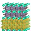 Halide perovskites have attracted tremendous interest due to their fascinating optoelectronic properties. Driven by the concerns of toxicity derived from lead and instability caused by organic components, researchers have turned to all-inorganic lead-free halide perovskites. However, compared to hybrid lead perovskite, lead-free compositions usually demonstrate poor crystallinity, low ordering, and high defects that suppress the performance of optoelectronic devices. Scientists now have deployed a new approach to grow all inorganic lead-free halide perovskites.
Mar 29th, 2018
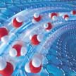 For most viscous liquids, the solid surface of surrounding channel walls poses friction resistance to the flowing liquid, causing a loss of velocity at the liquid/solid interface. As a result, for regular surfaces the energy required for nanofluidic applications is enormous because of the tremendous hydraulic resistance inside nanoscale conduits. A new technique to accurately measure the hydraulic resistance inside graphene nanofluidic channels makes increasing the efficiencies of most nanofluidic applications possible.
Mar 28th, 2018
 In new work employing the photostrictive effect, researchers have fabricated a flexible two-dimensional (2D) charge transfer molecular (sub-nanometer) nanosheet and observed a sizeable photostrictive effect of 5.7% with fast, sub-millisecond response; this is higher than that of some conventional ferroelectronics and polar semiconductors. This photostrictive effect arises from excess charge carriers induced lattice dilation and conformation change, which is higher than that of some conventional ferroelectronics and polar semiconductors.
Mar 27th, 2018
 Over the past few decades, researchers have developed various optical voltage sensing probes in order to overcome the highly invasive nature of electrode-based techniques. These voltage sensing mechanisms can be hampered by some combination of limitations including low sensitivity, slow kinetics, or heavy capacitive loading. This has motivated a group of researchers to explore DNA nanotechnology for developing novel optical voltage sensing nanodevices that convert a local change of electric potential into optical signals.They now report that a voltage can be read out in a nanopore with a dedicated F�rster resonance energy transfer (FRET) sensor on a DNA origami.
Mar 26th, 2018
 Researchers have used a few-layer antimonene nanosheet to demonstrate all optical modulation in optical signal processing. To utilize the saturable absorption property of few-layer antimonene, antimonene-decorated microfiber was employed as an optical saturable absorber that can allow for passive mode-locking, Q-switching and all-optical thresholding at the telecommunication band. These results may provide guidance for the application of antimonene and other Group VA mono-elemental 2D materials in ultra-short pulse generation and all optical thresholding with enhanced long term stability.
Mar 23rd, 2018
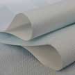 Imagine you are fast asleep in your bedroom when a fire breaks out somewhere else in your house. Fortunately, you have nanotechnology-enhanced wallpaper that detects the fire and automatically rings an alarm. Realizing this idea, scientists have developed a 'smart' wallpaper based on highly flexible fire-resistant inorganic paper embedded with ultralong hydroxyapatite nanowires that serve as the substrate and graphene oxide as the thermosensitive sensor.
Mar 21st, 2018
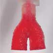 Imagine being able to print out healthy tissue with just a sample of a patient's own cells. While printed replacement human body parts might seem like science fiction, the use of 3D printing technologies for medical applications is a relatively new but rapidly expanding research field, although still quite a way from clinical application for treating patients. However, currently available bioinks cannot 3D print self-sustaining anatomic-size structures containing live cells. To overcome the limitations of existing bioinks, researchers have developed a highly printable bioink for fabricating large scale, cell-laden, bioactive scaffolds.
Mar 20th, 2018
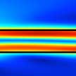
 Researchers report a simple method to facilitate the mass production of flexible photonic crystals (FPCs) with full-color grating properties. The nanoimprinted FPC structure is capable of displaying full-color grating properties because of the nano-hemispherical structures on its surface. This novel approach requires relatively inexpensive equipment and much less time than previous techniques. In addition, multiple anti counterfeiting applications can be easily implemented based on the polymer's intrinsic characteristics.
Mar 19th, 2018
 Subscribe to our Nanotechnology Spotlight feed