| Posted: Dec 23, 2015 |
Optoelectronic microprocessors built using existing chip manufacturing
(Nanowerk News) Using only processes found in existing microchip fabrication facilities, researchers at MIT, the University of California at Berkeley, and the University of Colorado have produced a working optoelectronic microprocessor, which computes electronically but uses light to move information.
|
|
Optical communication could dramatically reduce chips’ power consumption, which is not only desirable in its own right but essential to maintaining the steady increases in computing power that we’ve come to expect.
|
|
Demonstrating that optical chips can be built with no alteration to existing semiconductor manufacturing processes should make optical communication more attractive to the computer industry. But it also makes an already daunting engineering challenge even more difficult.
|
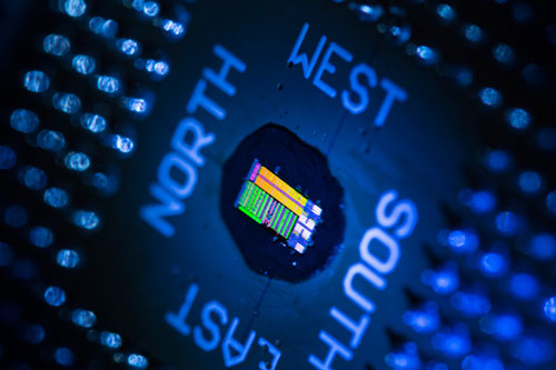 |
| Researchers have produced a working optoelectronic chip that computes electronically but uses light to move information. The chip has 850 optical components and 70 million transistors, which, while significantly less than the billion-odd transistors of a typical microprocessor, is enough to demonstrate all the functionality that a commercial optical chip would require. (Image: Glenn J. Asakawa)
|
|
“You have to use new physics and new designs to figure out how you take ingredients and process recipes that are used to make transistors, and use those to make photodetectors, light modulators, waveguides, optical filters, and optical interfaces,” says MIT professor of electrical engineering Rajeev Ram, referring to the optical components necessary to encode data onto different wavelengths of light, transmit it across a chip, and then decode it. “How do you build all the optics using only the layers out of a transistor? It felt a bit like an episode of ‘MacGyver’ where he has to build an optical network using only old computer parts.”
|
|
The project began as a collaboration between Ram, Vladimir Stojanovic, and Krste Asanovic, who were then on the MIT Department of Electrical Engineering and Computer Science faculty. Stojanovic and Asanovic have since moved to Berkeley, and they, Ram, and Miloš A. Popovic, who was a graduate student and postdoc at MIT before becoming an assistant professor of electrical engineering at Colorado, are the senior authors on a paper in Nature that describes the new chip ("Single-chip microprocessor that communicates directly using light").
|
|
They’re joined by 19 co-authors, eight of whom were at MIT when the work was done, including two of the four first authors: graduate students Chen Sun and Jason Orcutt, who has since joined IBM’s T. J. Watson Research Center.
|
|
Powering down
|
|
The chip has 850 optical components and 70 million transistors, which, while significantly less than the billion-odd transistors of a typical microprocessor, is enough to demonstrate all the functionality that a commercial optical chip would require. In tests, the researchers found that the performance of their transistors was virtually indistinguishable from that of all-electronic computing devices built in the same facility.
|
|
Computer chips are constantly shipping data back and forth between logic circuits and memory, and today’s chips cannot keep the logic circuits supplied with enough data to take advantage of their ever-increasing speed. Boosting the bandwidth of the electrical connections between logic and memory would require more power, and that would raise the chips’ operating temperatures to unsustainable levels.
|
|
Optical data connections are, in principle, much more energy efficient. And unlike electrical connections, their power requirements don’t increase dramatically with distance. So optical connections could link processors that were meters rather than micrometers apart, with little loss in performance.
|
|
The researchers’ chip was manufactured by GlobalFoundries, a semiconductor manufacturing company that uses a silicon-on-insulator process, meaning that in its products, layers of silicon are insulated by layers of glass. The researchers build their waveguides — the optical components that guide light — atop a thin layer of glass on a silicon wafer. Then they etch away the silicon beneath them. The difference in refractive index — the degree to which a material bends light — between the silicon and the glass helps contain light traveling through the waveguides.
|
|
Conflicting needs
|
|
One of the difficulties in using transistor-manufacturing processes to produce optical devices is that transistor components are intended to conduct electricity, at least some of the time. But conductivity requires free charge carriers, which tend to absorb light particles, limiting optical transmission.
|
|
Computer chips, however, generally use both negative charge carriers — electrons — and positive charge carriers — “holes,” or the absence of an electron where one would be expected. “That means that somewhere in there, there should be some way to block every kind of [carrier] implant that they’re doing for every layer,” Ram explains. “We just had to figure out how we do that.”
|
|
In an optoelectronic chip, at some point, light signals have to be converted to electricity. But contact with metal also interferes with optical data transmission. The researchers found a way to pattern metal onto the inner ring of a donut-shaped optical component called a ring resonator. The metal doesn’t interact with light traveling around the resonator’s outer ring, but when a voltage is applied to it, it can either modify the optical properties of the resonator or register changes in a data-carrying light signal, allowing it to translate back and forth between optical and electrical signals.
|
|
On the new chip, the researchers demonstrated light detectors built from these ring resonators that are so sensitive that they could get the energy cost of transmitting a bit of information down to about a picojoule, or one-tenth of what all-electronic chips require, even over very short distances.
|
|
The new paper “certainly is an important result,” says Jagdeep Shah, a researcher at the U.S. Department of Defense’s Institute for Defense Analyses who, as a program director at the Defense Advanced Research Project Agency, initiated the program that sponsored the researchers’ work. “It is not at the megascale yet, and there are steps that need to be taken in order to get there. But this is a good step in that direction.”
|
|
“I think that the GlobalFoundries process was an industry-standard 45-nanometer design-rule process,” Shah adds. “I don’t think that there need be any concern that there’s any foundry that can’t make these things.”
|

