| Feb 20, 2020 |
Scientists develop new method to isolate atomic sheets and create new materials(Nanowerk News) Two-dimensional materials from layered van der Waals (vdW) crystals hold great promise for electronic, optoelectronic, and quantum devices, but making/manufacturing them has been limited by the lack of high-throughput techniques for exfoliating single-crystal monolayers with sufficient size and high quality. |
| Columbia University researchers report in Science ("Disassembling 2D van der Waals crystals into macroscopic monolayers and reassembling into artificial lattices") that they have invented a new method – using ultraflat gold films – to disassemble vdW single crystals layer by layer into monolayers with near-unity yield and with dimensions limited only by bulk crystal sizes. |
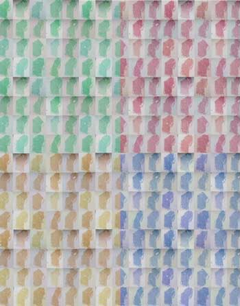 |
| This image shows atomically thin semiconductor wafers (MoS2 monolayers, lateral dimension of each panel ~ 1cm, wafer thickness of only ~0.7 nm). The researchers obtained these monolayers from layer-by-layer exfoliation of a MoS2 single crystal using the gold tape method. The images have been Photoshop-processed for artistic appeal. (Image: Fang Liu, Qiuyang Li, Andrew Schlaus, Wenjing Wu, Yusong Bai, and Kihong Lee/Columbia University ) |
| The monolayers generated using this technique have the same high quality as those created by conventional “Scotch tape” exfoliation, but are roughly a million times larger. The monolayers can be assembled into macroscopic artificial structures, with properties not easily created in conventionally grown bulk crystals. |
| For instance, layers of molybdenum disulfide can be aligned with each other so that the resulting stack lacks mirror-symmetry and as a result demonstrates strongly nonlinear optical response, where it absorbs red light and emits ultraviolet light, a process known as second harmonic generation. |
| “This approach takes us one step closer to mass production of macroscopic monolayers and bulk-like artificial materials with controllable properties,” says co-PI James Hone, Wang Fong-Jen Professor of Mechanical Engineering. |
| The discovery 15 years ago that single atomic sheets of carbon – graphene – could be easily separated from bulk crystals of graphite and studied as perfect 2D materials was recognized with the 2010 Nobel prize in physics. |
| Since then, researchers worldwide have studied properties and applications of a wide variety of 2D materials, and learned how to combine these layers into stacked heterostructures that are essentially new hybrid materials themselves. |
| The original scotch tape method developed for graphene, which uses an adhesive polymer to pull apart crystals, is easy to implement but is not well-controlled and produces 2D sheets of limited size—typically tens of micrometers across, or the size of a cross-section of a single strand of hair. |
| A major challenge for the field and future manufacturing is how to scale up this process to much larger sizes in a deterministic process that produces 2D sheets on demand. The dominant approach to scaling up the production of 2D materials has been the growth of thin films, which has yielded great successes but still faces challenges in material quality, reproducibility, and the temperatures required. |
| Other research groups pioneered the use of gold to exfoliate large 2D sheets, but have used approaches that either leave the 2D sheets on gold substrates or involve intermediate steps of evaporating hot gold atoms that damage the 2D materials. |
| “In our study, we were inspired by the semiconductor industry, which makes the ultrapure silicon wafers used for computer chips by growing large single crystals and slicing them into thin disks,” says the lead PI Xiaoyang Zhu, Howard Family Professor of Nanoscience in Columbia’s department of chemistry. “Our approach does this on the atomic scale: we start with a high-purity crystal of a layered material and peel off one layer at a time, achieving high-purity 2D sheets that are the same dimensions as the parent crystal.” |
| The researchers took their cue from the Nobel prize-winning scotch tape method and developed an ultraflat gold tape instead of the adhesive polymer tape. The atomically flat gold surface adheres strongly and uniformly to the crystalline surface of a 2D material and disassembles it layer by layer. The layers are the same size and dimension as the original crystal – providing a degree of control far beyond what is achievable using scotch tape. |
| “The gold tape method is sufficiently gentle that the resulting flakes have the same quality as those made by scotch tape technique,” says postdoctoral scholar Fang Liu, the lead author on the paper. “And what is especially exciting is that we can stack these atomically thin wafers in any desired order and orientation to generate a whole new class of artificial materials.” |
| The work was carried out in the Center for Precision Assembly of Superstratic and Superatomic Solids, a Materials Science and Engineering Research Center funded by the National Science Foundation and led by Hone. The research project used shared facilities operated by the Columbia Nano Initiative. |
| Motivated by recent exciting advances in “twistronics,” the team is now exploring adding small rotation between layers in these artificial materials. In doing so, they hope to achieve on a macro-scale the remarkable control over quantum properties such as superconductivity that have recently been demonstrated in micrometer-sized flakes. |
| They are also working to broaden their new technique into a general method for all types of layered materials, and looking at potential robotic automation for large scale manufacturing and commercialization. |
| Source: Columbia University |
|
Subscribe to a free copy of one of our daily Nanowerk Newsletter Email Digests with a compilation of all of the day's news. |

