| Feb 03, 2023 |
Two/quasi-two-dimensional perovskite-based heterostructures: Construction, properties and applications
(Nanowerk News) Van der Waals heterostructures integrated from various two-dimensional (2D) layered materials provide fundamental building blocks for optoelectronic devices with novel functionalities, such as photovoltaic solar cells, light emitting diodes (LEDs) and photodetectors.
|
|
Especially, two-dimensional and quasi-two-dimensional perovskites (abbreviated both of them as 2D perovskites hereafter) exhibit unique properties, such as large exciton binding energy, high photoluminescence quantum efficiency, large oscillator strengths and long carrier diffusion length, and thus are emerging candidates for next-generation optoelectronic devices.
|
|
To this end, heterostructures incorporating distinct layered 2D perovskites with other layered or non-layered materials can introduce unique optical and optoelectronic properties and vastly expand the potential functionalities and applications of the heterostructures.
|
|
Publishing in the journal IJEM ("Two/Quasi-two-dimensional perovskite-based heterostructures: construction, properties and applications"), the team led by researchers based at the Huazhong University of Science and Technology have summarized the recent achievements of 2D/quasi-2D perovskite-based heterostructures to facilitate the discovery of unexplored phenomena and open up a new range of optoelectronic applications.
|
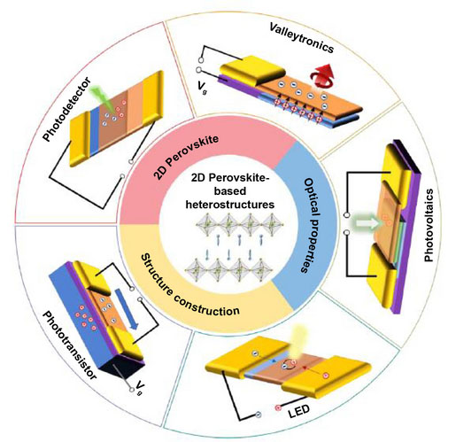 |
| In this article, the structure and physical properties of 2D perovskites will be first highlighted. The construction and characterizations of 2D perovskite-based heterostructures as well as the basic optical properties of the constructed heterostructures will then be illustrated. Furthermore, the potential applications of 2D perovskite-based heterostructures in photovoltaic devices, light-emitting diodes, photodetectors, phototransistors and valleytronic devices will be demonstrated. Finally, the current challenges and propose further research directions in the field of 2D perovskite-based heterostructures will be discussed. (Image: Haizhen Wang, Yingying Chen and Dehui Li)
|
|
The team introduced the structure and physical properties of 2D/quasi-2D perovskites and then discussed the construction and characterization of 2D/quasi-2D perovskite-based heterostructures and also highlighted the prominent optical properties of the constructed heterostructures. Further, the potential applications of 2D/quasi-2D perovskite-based heterostructures in photovoltaic devices, light emitting devices, photodetectors/phototransistors and valleytronic devices were demonstrated. The challenges and perspectives in the field of 2D perovskites-based heterostructures were also outlined.
|
|
The lead researcher, Professor Dehui Li, commented, "The rich electronic and optical physics offered by 2D perovskites renders them to be very promising for optoelectronic applications. The electronic structure of 2D perovskites can be efficiently modulated by changing the layer number n value, substituting halide anions and incorporating organic chains, which further modifies their optical performances, bringing both advantages and disadvantages for optoelectronic applications."
|
|
"However, the synthesis of pure phase quasi-2D perovskites and heterostructures on a large scale in a controllable manner is still lacking. In this review, we summarized all developed methods to prepare 2D perovskite and heterostructures, which would be helpful to explore new strategies for material preparation."
|
|
Heterostructure construction lay the foundation for optoelectronic device architectures and applications. Various techniques have been developed to build 2D perovskite heterostructures, including dry transfer, solution synthesis and vapor deposition. Besides, optical spectra, phase identification and surface morphology characterization are the common methods to characterize the constructed heterostructures.
|
|
Co-first author Dr. Haizhen Wang said, "Optical property is one fascinating functional aspect of 2D perovskite-based heterostructures, which not only inherit the basic physical properties of 2D perovskites but also show rich new photophysics that does not exhibit in each constituent material."
|
|
Thus, 2D perovskite-based heterostructures provide an ideal platform to study the charge/energy-transfer processes, ion migration-induced optical properties and nonlinear optical effects. Nevertheless, studies on those aspects remain at a preliminary stage and further investigations are called for.
|
|
Co-first author Ph.D. student Yingying Chen said, "2D perovskites can be stacked with other materials to establish heterostructures with different band alignments, which can be type I or type II based on different constituents in heterostructures leading to different optoelectronic applications."
|
|
In this review, performances in photovoltaic devices, photodetectors, light-emitting devices, phototransistors and valleytronic devices based on various 2D perovskite heterostructures have been sorted and discussed.
|
|
Prof. Dehui Li said: "The excellent optical and optoelectronic properties of 2D perovskite-based heterostructures have led to a wide range of applications in optics and optoelectronics. However, many problems are still encountered at this stage, which include the rational synthesising pure phase 2D perovskites and their heterostructures on large scale in a controllable manner, deeply understanding their fundamental physical properties as well as fully exploring their potential novel optoelectronic applications."
|
|
"We believe that more 2D perovskite-based heterostructures with novel functionalities will be constructed taking advantage of the great flexibility in composition, structure and properties of 2D perovskites."
|

