| Jun 23, 2025 |
Plasmonic metasurfaces boost brightness in 2D semiconductor light emitters
A new metasurface design greatly improves light emission in atomically thin materials, offering a path to low-power, flexible, high-brightness display technologies.
(Nanowerk News) Van der Waals materials (vdWMs) are an exciting group of ultra-thin materials—just a few atoms thick. They’re attracting attention in both research and industry because they are flexible and have better electrical and light-based (optoelectronic) properties than traditional silicon materials. Semiconductor companies like TSMC and Intel are now putting major effort into using these 2D semiconductors in future devices.
|
|
But there’s a problem: even though these materials are promising, using them in devices that emit light—like LEDs or display panels—has been difficult. The main obstacles are that they don’t emit light efficiently (low quantum yield) and they’re hard to use over large areas.
|
|
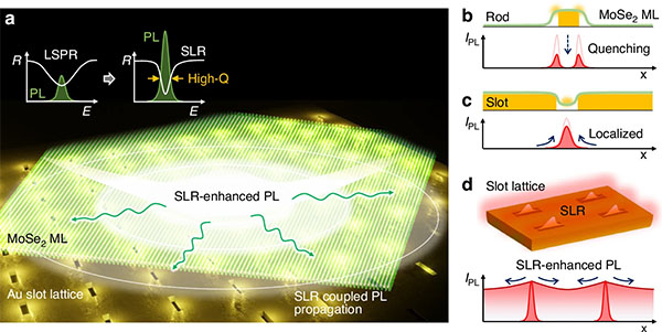
To tackle this, a research team led by Prof. Kyoung-Duck Park and Prof. Junsuk Rho at POSTECH, along with Prof. Vasily Kravtsov at ITMO University, created a new kind of surface called a plasmonic metasurface. This surface is combined with 2D materials and solves key problems found in older designs, like poor light emission and overly localized effects (only enhancing light in very tiny regions).
|
 |
| Conceptual diagram illustrating Babinet’s principle and surface lattice resonance (SLR) effects. (Image: Light: Science & Applications, CC BY)
|
|
Their study was published in Light: Science & Applications ("High momentum two-dimensional propagation of emitted photoluminescence coupled with surface lattice resonance").
|
The team focused on solving a key issue in making low-power, flexible displays: how to get more light out of monolayer semiconductors (just one layer of atoms). Until now, researchers have tried using tiny metal antennas to enhance light emission. But these metal antennas come with two major downsides:
- A lot of energy is lost as heat where the metal touches the semiconductor.
- The light enhancement only happens in very small areas—about 100 square nanometers—and is spread unevenly.
|
|
The team overcame these issues by designing a metasurface made of hollow slot antennas. These were based on two principles from physics: Babinet’s principle and Rayleigh’s anomaly. This design helps the 2D material emit more light by increasing the rate of radiative decay (how fast energy is released as light) and allowing light to be generated over a wider area. They tested it on a monolayer of molybdenum diselenide (MoSe₂).
|
|
Instead of enhancing light only in tiny regions, the metasurface takes advantage of a phenomenon called surface lattice resonance (SLR). This creates a much broader and stronger enhancement effect across the surface. The result is a large-area, bright light emission that uses very little power. In some places, light emission was boosted by up to 1,600 times. To study how this light spreads and what direction it goes in, the team used special spectroscopic tools that measure light depending on angle and location.
|
|
The researchers believe this work points toward a new era of display technology. As they put it, people are now looking beyond traditional large screens like IMAX, aiming for immersive experiences on a massive scale—such as the Las Vegas Sphere. These future displays need to be flexible, use little power, emit very bright light, and work over large areas. This new design moves the field closer to making that possible with 2D materials.
|
|
They also highlighted the novelty of their method: by bringing together Babinet’s principle and surface lattice resonances in a new metasurface design, they’ve solved persistent problems in how light interacts with these thin materials. They believe this platform could be central to future high-brightness displays and light-based communication systems.
|
|
This development is considered a major step toward changing how we design and use optoelectronic and display technologies in everyday life.
|

