| Feb 15, 2013 |
Development of a graphene transistor with a new operating principle
|
|
(Nanowerk News) Naoki Yokoyama, Shu Nakaharai, and others, Collaborative Research Team Green Nanoelectronics Center (GNC), the Nanoelectronics Research Institute (NeRI) of the National Institute of Advanced Industrial Science and Technology (AIST) and Shinichi Ogawa and others, NeRI, AIST, have developed a graphene transistor with a new operating principle, in collaboration with Innovation Center for Advanced Nanodevices (ICAN), AIST, and Kazuhito Tsukagoshi, the International Center for Materials Nanoarchitectonics (MANA) of the National Institute for Materials Science (NIMS).
|
|
In the developed transistor, two electrodes and two top gates are placed on graphene and graphene between the top gates is irradiated with a helium ion beam to introduce crystalline defects. Gate biases are applied to the two top gates independently, allowing carrier densities in the top-gated graphene regions to be effectively controlled. An electric current on/off ratio of approximately four orders of magnitude was demonstrated at 200 K (approximately -73 °C). In addition, its transistor polarity can be electrically controlled and inverted, which to date has not been possible for transistors. This technology can be used in the conventional production technology of integrated circuits based on silicon, and is expected to contribute to the realization of ultra-low-power-consumption electronics by reducing operation voltage in future.
|
|
Details of this technology were presented at the 2012 International Electron Devices Meeting (IEDM 2012) held in San Francisco, U.S.A., from December 10 to 12, 2012.
|
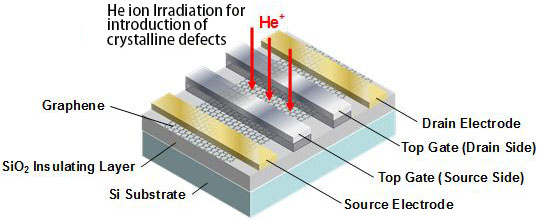 |
| Schematic illustration of a graphene transistor prototype.
|
|
Social Background of Research
|
|
In recent years, the increase in power consumption associated with the spread of mobile information terminals and the progress in IT devices has become a concern. Societal demand for reduction of the power consumed by electronic information devices is increasing. Although attempts at reducing the power consumed by large-scale integrated circuits (LSIs) have been advanced, the conventional transistor structure is considered to have inherent limits. Meanwhile, electron mobility of graphene, which represents the ease of electron movement, is at least 100 times larger than that of silicon. It is also expected that graphene can be used to resolve the problems of the inherent limits of silicon and other materials. Therefore, graphene has the potential to remove the obstacle to reducing the power consumed by LSIs, and it is expected that graphene will be used as a material for ultra-low-power-consumption transistors of the post-silicon age that utilize new functional atomic films.
|
|
However, when graphene is used in a switching transistor, electric current cannot be sufficiently interrupted, because graphene has no band gap. Also, although there is technology for forming band gaps, electron mobility decreases when the band gap required for switching is formed. Therefore, a graphene transistor with a new operating principle that can perform the switching operation effectively with a small band gap is required.
|
|
History of Research
|
|
GNC was established in April 2010 to carry out a project adopted by FIRST operated by the Cabinet Office and the Japan Society for the Promotion of Science. GNC is comprised of AIST researchers and corporate researches from five companies (Fujitsu Laboratories, Ltd.; Toshiba Corporation; Hitachi, Ltd.; Renesas Electronics Corporation; and Ulvac, Inc.). Based on a framework of research support from Tsukuba Innovation Arena, NeRI and ICAN of AIST and MANA of NIMS have been conducting collaborative research at GNC for electronics applications of graphene since FY2010.
|
|
This research was supported by "Development of Core Technologies for Green Nanoelectronics" project (Core Researcher: Naoki Yokoyama) of FIRST.
|
|
Details of Research
|
|
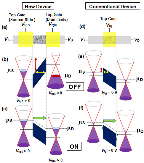
The operating principle of the newly developed graphene transistor is shown in Figs 1(a) to 1(c). In order to create a transport gap in graphene of the channel between the two top gates, a helium ion microscope was used to irradiate helium ions at a density of 6.9 x 10¹⁵ ions/cm2 to introduce crystalline defects. The energy band of the graphene on both sides of the channel can be modulated by electrostatic control by applying biases to the top gates. The polarity of the carriers in graphene can be changed between n-type and p-type, depending on the polarity of the biases applied to the top gates. When the polarities on both sides of the channel differ, the transistor is in an off state (Fig. 1(b)). When the polarities are the same, the transistor is in an on state (Fig. 1(c)). When a conventional transistor (Figs. 1(d) to 1(f)) is in an off state, carrier transport is blocked by a barrier formed on the source- or drain-side end of the channel having the transport gap. However, as shown in Fig. 1(e), the leak current of the transistor in the off state is large, because only a small barrier is formed. Meanwhile, as Fig. 1(b) shows, the transport gap in the developed transistor works as a barrier larger than that of conventional transistors (Fig. 1(e)) and blocks charge transfer. As a result, it is possible to obtain a superior off state to that of conventional transistors.
|
|
In the developed transistor, the length of channel, in which mobility deteriorates usually, can be reduced to the length shorter than that of conventional transistors. In addition, because the developed transistor can achieve an efficient off state with a small transport gap, the transport gap can be made smaller than that of conventional devices. Due to these properties, the on/off operation of the transistor can be performed more rapidly than with conventional transistors, and thus it is believed that an LSI with lower power consumption can be realized by reducing the operation voltage of the circuit. In addition, the transistors can be produced using the conventional fabrication technology for silicon integrated circuits, such as lithography, deposition, and doping processes, and can also be easily produced in wafer scale.
|
 |
| Figure 1: Operating principles of the new graphene transistor and conventional transistors.
|
|
In order to demonstrate the transistor operation of the new operation principle, a transistor was fabricated by forming source and drain electrodes and a pair of top gates on a single-layer graphene isolated from graphite. An appropriate dose of helium ions was applied between the top gates to make a helium ion irradiated channel (Fig. 2, blue dotted line), and the outer unnecessary graphene was irradiated with a heavy dose of helium ions to make it an insulator (Fig. 2, red dotted line). As a result, the transistor channel is 20 nm in length and 30 nm in width.
|
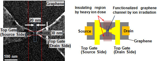 |
| Figure 2: Helium ion microscope image and schematic illustration of the prototype device
|
|
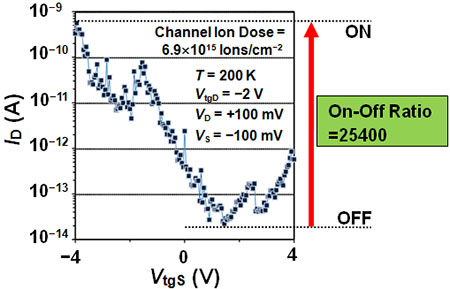
On/off operation of the fabricated transistor was performed at the low temperature of 200 K (approximately -73 °C). The source and drain terminals were applied with biases of -100 mV and +100 mV, respectively. The gate bias of the drain-side gate was fixed at -2 V, and that of the source-side gate was swept from -4 V to +4 V and the electric current flowing between the source and drain electrodes was measured. An on/off ratio of approximately four orders of magnitude was observed (Fig. 3).
|
 |
| Figure 3: On/off ratio of electric current of the new graphene transistor
|
|
In the developed transistor, the on state or off state is controlled according to whether the polarities of the voltages applied to the two top gates are the same or different. Therefore, by fixing one gate bias and changing its polarity, it is possible to control whether the transistor operation by sweeping the other gate voltage is n-type or p-type. In the present experiment, voltages of -100 mV and +100 mV were applied to the source and drain terminals, respectively. The relation between the source-drain current and the bias of the source-side gate when the gate voltage of the drain-side, VtgD, is fixed to be positive (Fig. 4(a)), is shown in Fig. 4(b). A logarithmic plot of the same data is shown in Fig. 4 (c). Here, when the gate voltage of the source-side is negative, the transistor is off, and when it is positive, the transistor is on. So it operates as an n-type transistor. Meanwhile, the relation between the source-drain current and the bias of the source-side gate when the gate voltage of the drain-side is negative (Fig. 4(d)), is shown in Figs 4(e) and 4(f). In this case, when the gate voltage of the source-side is negative, the transistor is on, and when positive, the transistor is off. So it operates as a p-type transistor. In other words, it was actually demonstrated that the polarity of a single transistor can be inverted by electrostatic control.
|
|
The transistor polarity of conventional silicon transistors is determined by the type of ion for doping, so it is not possible to change the polarity once a circuit is formed. However, because the polarity of the developed transistor can be electrostatically controlled, it is possible to realize an integrated circuit whose circuit structure can be electrically changed.
|
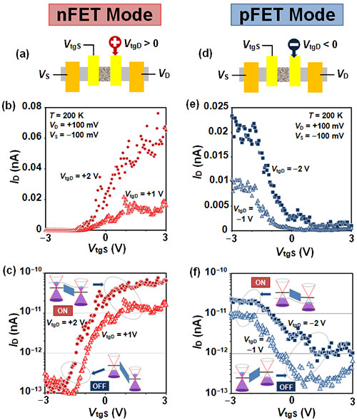 |
| Figure 4: Demonstration of transistor operation in which the transistor polarity was electrically inverted. VtgD is the gate voltage of the drain-side
|
|
Future Plans
|
|
The researchers are aiming to realize CMOS operation in which transistor polarities can be changed through electrical control. They are also aiming to create a device prototype using a large-scale wafer with graphene synthesized by the CVD method (chemical vapor-phase deposition method). At the same time, efforts to achieve higher-quality graphene will be made in order to improve the on/off ratio of electric current at room temperature and carrier mobility.
|

