| Posted: Mar 29, 2018 |
Single crystalline epitaxy of all inorganic lead-free halide perovskite paves the way for high-performance electronics |
| (Nanowerk Spotlight) Halide perovskites have attracted tremendous interest due to their fascinating optoelectronic properties. Driven by the concerns of toxicity derived from lead and instability caused by organic components, researchers have turned to all-inorganic lead-free halide perovskites. |
| However, compared to hybrid lead perovskite, lead-free compositions usually demonstrate poor crystallinity, low ordering, and high defects that suppress the performance of optoelectronic devices. |
| In a recent article featured as the inside front cover of Advanced Materials Interfaces ("Unlocking the Single-Domain Epitaxy of Halide Perovskites"), a research team composed of scientists from Michigan State University and University of Michigan have deployed a new approach to grow all inorganic lead-free halide perovskites. |
| "Epitaxial growth has long since revolutionized the study of many electronic materials including silicon, oxide perovskites, and III-V semiconductors," Richard Lunt, an Associate Professor at Department of Chemical Engineering and Materials Science, Michigan State University who has supervised the project, tells Nanowerk. "There is very little known about the epitaxial growth of halide perovskites, but these exciting materials hold enormous potential. This has motivated us to explore this entirely new research area." |
| Inspired by the research on oxide perovskite and III-V semiconductor, Lunt’s research group has successfully developed a reactive co-deposition method to grow single domain epitaxy of all inorganic lead-free halide perovskite with monolayer control. Moreover, they are able to precisely control the phase of the epitaxial halide perovskite by adjusting the stoichiometry and therefore modulate the optoelectronic properties. |
| In-situ real-time monitoring of the phase transition from CsSnBr3 to CsSn2Br5. |
| Based on the precise manipulation of phase and monolayer thickness, the team has fabricated the first epitaxial multilayer quantum well system incorporating a halide perovskite. Such a demonstration could lead to their application in various advanced electronics including lasers, photodetectors, and transistors. |
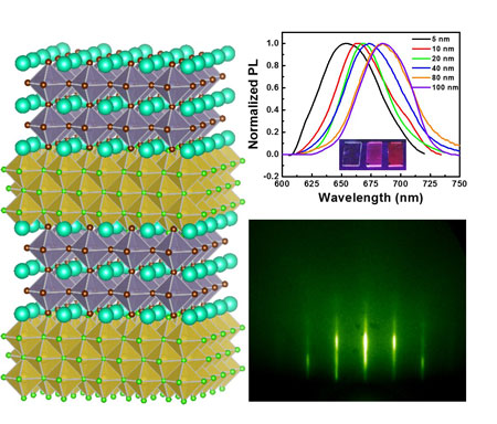 |
| Figure 1. Quantum Well Systems: Scheme, Photoluminescence Spectrum, Photograph, and RHEED Pattern. |
| "A key factor for epitaxial growth is to control the lattice misfit between the substrates and epitaxy," says Lili Wang, a Research Associate in Lunt’s lab who has led the experimental part of this work. "In our current research, we use low-cost alkali metal halide salts as substrates. Previously, we had developed a method to control the lattice misfit by alloying different types of alkali metal halide salts." |
| By deploying this alloy approach, the researchers can achieve near-zero lattice misfit and adjust the lattice constant of their substrates. This provides a lot of flexibility on the selection of substrates. |
| For the sake of fabricating devices, they further developed an epitaxial lift-off method to transfer the epitaxial film to any substrate of interest. |
| The solar cell device fabricated with the transferred single crystalline film as the absorber layers demonstrated both higher photocurrent and photovoltage than the control devices fabricated with amorphous films thanks to the improved crystallinity and film ordering achieved by epitaxial growth. |
| Their devices suggested that the power conversion efficiency of devices fabricated with this halide perovskite composition is likely to exceed at least 10%. |
| "More importantly, after transferring we are able to reuse the substrates for the next round of epitaxial growth. It can further reduce the cost of this method," Wang emphasizes. |
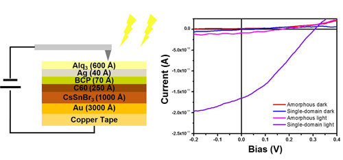 |
| Figure 2. Photovoltaic Application: Scheme of Devices and Current-Voltage Measurement. |
| Lunt concludes, "We believe halide perovskite have the potential to revolutionize various fields including solar photovoltaics and many other high end optoelectronics." |
|
Provided by the Molecular and Organic Excitonics Lab at Michigan State University as a Nanowerk exclusive.
|

Become a Spotlight guest author! Join our large and growing group of guest contributors. Have you just published a scientific paper or have other exciting developments to share with the nanotechnology community? Here is how to publish on nanowerk.com. |
