| Posted: Sep 29, 2015 |
Ultrahigh-resolution digital image sensor achieves pixel size of 50 nm |
| (Nanowerk Spotlight) The digital image sensor, widely used in digital cameras and other modern vision information technologies, is a device that converts an optical image into an electronic signal. Existing digital image sensors can be divided into two categories: charge-coupled device (CCD) and complementary metal-oxide semiconductor (CMOS). The structures of CCD and CMOS are complex and each pixel contains multiple parts. |
| With the advance of microelectronics, the pixel size of image sensor keeps decreasing to improve the sensor resolution. Currently, the CCD pixel size and CMOS pixel size can be fabricated as small at 1.43 microns and 1.12 microns, respectively. However, it is extremely difficult to further decrease the pixel size due to the limitations of the silicon base material that is used and current sensor architecture. |
| The main pixel structure of current CMOS image sensor uses silicon p-n photodiodes as the core part with a pixel size of several micrometers. However, as the size of the photodiode decreases, their performance also decreases. Active CMOS image sensors therefore employ FET amplifiers to enhance the signal coming from the p-n photodiodes. This structure increases the complexity of the device and requires more space for integrating one pixel. |
| To overcome the pixel size limitation of existing digital image sensors, both new materials with enormous photoelectric properties and novel device architectures are required. But the benefits will be huge. Ultra-high resolution will bring revolutionary changes in photography, telecommunication, and machine-vision, etc. Furthermore, ultra-small pixels have a size smaller than the wavelength of visible light, and thus can serve as an effective tool to explore the interaction between light and matter. |
| In a recent paper in Advanced Materials ("An Ultrahigh-Resolution Digital Image Sensor with Pixel Size of 50 nm by Vertical Nanorod Arrays"), researchers are reporting a new, ultra-high resolution nanorod digital image sensor (NDIS) which is fabricated by sandwiching vertically aligned zinc oxide nanorod arrays between orthogonal top and bottom nanostripe electrodes. |
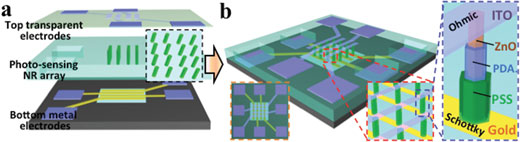 |
| Design and fabrication of the NDIS. a) The illustrations of the design and the structure of an NDIS with vertical nanorod (NR) pixels interconnected by orthogonal top and bottom nanostripe electrodes. In the right dashed-line rectangle, uniform, and vertical NR arrays as the 3D pixels are schematically shown in a titled view. b) Architecture of the assembled NDIS with electrically addressable 4 × 4 NR pixels. The top view of the device is shown in the orange dashed-line rectangle. An enlarged view of a 3D NR pixel (red dashed line highlighted) with a cross-sectional illustration (blue dashed line highlighted) that indicates the key designs of the NR pixels: the vertical ZnO NR as the core material for each pixel; the PDADMAC (PDA) and the PSS as the surface functionalization layers coated on the NR sequentially; the ITO as the top transparent electrodes forming Ohmic contact and the gold as the bottom electrodes forming Schottky contact. (Reprinted with permission by Wiley-VCH Verlag) |
| "The most important application of the NDIS is as a next-generation digital image sensor with ultra-high resolution, well beyond the limit of existing techniques," Jinhui Song, Assistant Professor in the Department of Metallurgical & Materials Engineering Center for Materials for Information Technology at The University of Alabama, tells Nanowerk. "Unlike existing CCD or CMOS sensors with their complexity, the NDIS has a simple structure and ultra-high resolution by taking advantage of the novel properties of nanomaterials and a unique device design." |
| Song notes that the team achieved two significant breakthroughs for the fabrication of ultra-high resolution digital image sensors. |
| Firstly, they defined and invented a new basic element of digital integrated circuit, the photo-effect transistor (PET). |
| "The PET has an extremely simple architecture of two terminal electrodes and it can sense photo intensity and amplify the photoelectric signal," explains Song. "Existing digital image sensor pixels, such as CMOS, have two units – a photodiode and a field-effect transistor (FET) – to realize the photo sensing function. The photodiode, which occupies most of the area of the pixel, senses photo intensity and converts it into an electrical signal. The FET amplifies the electrical signal coming from the sensor." |
| By contrast, he points out, the simple two terminal PET combines both photo-sensing and electrical amplification functions in one unit. This means that one PET could function as an entire pixel, which significantly reduces the pixel complexity and enables the sensor pixel miniaturization. |
| Secondly, as a proof of concept, the researchers fabricated an ultra-high resolution digital image sensor with a pixel size of 50 nanometers by using vertical photoelectric nanorod arrays as 3D PET pixels. |
| "This innovative sensor structure greatly decreases the planar area of each pixel yet still maintains their excellent optoelectronic response," says Song. |
| In their work, Song and his co-author Chengming Jiang, a PhD student in his group, conducted a comprehensive study of the optoelectronic properties of a nanorod PET pixel with regard to size, surface functionalization, and Schottky barrier. As a result, they were able to increase the nanorod pixel on-off ratio, photoelectric response speed, and photo response spectra. |
| Overall, the resolution of this nanorod digital image sensor is two orders higher than that of existing CCD and CMOS digital image sensor techniques. |
| Going forward, the scientists plan to increase the pixel number to 100,000 in order to realize a large-scale digital image sensor with unprecedented high resolution. |
| Another issue that they will work on is the NDIS' light sensing response time of 0.1s – which is considerably slower than the fastest values (10-8s) that have been reported for ZnO nanomaterials. |
| "This might be attributed to the crystal quality of the ZnO nanorods and could be improved by growth optimization," Song suggests. |
| Furthermore, although the ZnO nanorod pixel has a strong absorption from 250nm to 450nm, through doping or surface modification the response spectra of ZnO nanorods could be extended to a longer wavelength to cover the entire visible spectra and even near-infrared. |
 By
Michael
Berger
– Michael is author of four books by the Royal Society of Chemistry:
Nano-Society: Pushing the Boundaries of Technology (2009),
Nanotechnology: The Future is Tiny (2016),
Nanoengineering: The Skills and Tools Making Technology Invisible (2019), and
Waste not! How Nanotechnologies Can Increase Efficiencies Throughout Society (2025)
Copyright ©
Nanowerk LLC
By
Michael
Berger
– Michael is author of four books by the Royal Society of Chemistry:
Nano-Society: Pushing the Boundaries of Technology (2009),
Nanotechnology: The Future is Tiny (2016),
Nanoengineering: The Skills and Tools Making Technology Invisible (2019), and
Waste not! How Nanotechnologies Can Increase Efficiencies Throughout Society (2025)
Copyright ©
Nanowerk LLC
|

Become a Spotlight guest author! Join our large and growing group of guest contributors. Have you just published a scientific paper or have other exciting developments to share with the nanotechnology community? Here is how to publish on nanowerk.com. |
