Showing Spotlights 177 - 184 of 625 in category All (newest first):
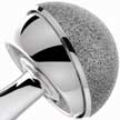 The implantation of orthopaedic devices is associated with a high risk of post-operative complications that increases substantially with each revision surgery. Researchers now have proposed a two-pronged strategy to address this outstanding clinical problem by combatting infections and providing bioactivity for titanium implants. Their nanostructured surfaces simultaneously are highly antimicrobial as well as bioactive - the goal of combining both functions without inducing cytotoxicity has thus far proved elusive.
Sep 4th, 2017
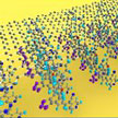
 Due to their unique interlayer coupling and optoelectronic properties, van der Waals heterostructures are of considerable interest for the next generation nanoelectronics. Conventional 2D heterostructures usually are composed of two layers of opposite charge carrier type using inorganic materials. One of the challenges when creating 2D heterostructures is the painstaking stacking of the individual components on top of each other. Researchers have now found, for the first time, that there can also be charge transfer (CT) induced interfacial coupling between two different pairs of organic CT layers.
Aug 23rd, 2017
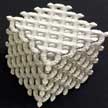
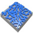 Quasi-periodic and random patterns in nature can exhibit extraordinary functions, such as iridescent color in bird wings, strong adhesion in gecko feet, and water repellency from lotus leaves. However, nature-inspired 3D nanostructures can be prohibitively expensive to make using modern nanoscale manufacturing processes. In new work, researchers a design approach integrated with scalable nanomanufacturing that can rapidly optimize and fabricate quasi-random photonic nanostructures.
Aug 1st, 2017
 Chiral metamaterials with strong chiroptical properties are an interesting new platform for optical signal modulation. Although plasmonic super chiral fields have been successfully applied to detect the chiral structures of proteins, it has remained challenging to detect the structural handedness of drug molecules due to their small size and thinner film adsorbed on the surface of metamaterials. Researchers now have reported a new type of plasmonic chiral metamaterial by stacking two layers of identical achiral gold nanohole arrays into moire patterns.
Jul 25th, 2017
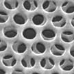
 Three-dimensional (3D) printing, also known as additive manufacturing, is a fabrication method that creates structures from digital models. Unlike conventional fabrication methods, 3D printing processes are bottom-up fabrication methods which are based on the incremental addition of layers of materials. Recently, 3D-printing has also been shown to be advantageous to catalytic applications since a printing approach can achieve better control of the fine structure of the target material. It is expected that 3D printing fabrication will provide new solutions for preparing catalysts with new structures in a more economical and energy-efficient way.
Jun 27th, 2017
 Sometimes nanoscale diamonds contain a specific type of impurity: a single nitrogen atom where a carbon atom should be, with an empty space right next to it, resulting from a second missing carbon atom. This nitrogen-vacancy (NV) impurity gives each nanodiamond special optical and electromagnetic properties. Nitrogen vacancy centers in nanodiamonds require a method to manipulate their electron spin orientations physically. Recent work demonstrates a general active NV system: Nanodiamond swimmers that self-propel.
Jun 20th, 2017
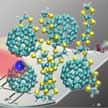
 Since the early days of molecular electronics, tremendous progress has been achieved both theoretically and experimentally by scientists and engineers who were fascinated by intriguing physical, chemical phenomena, and potential device applications of molecular junctions. In a recent paper, scientists review recent experimental efforts for pursuing high-yield functional molecular devices, in which a bundle of molecules (the contacted molecules number more than 1000) is contained in a junction.
Jun 14th, 2017
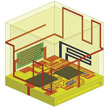 Researchers have demonstrated a fully integrated and packaged wireless sensor for environmental monitoring applications. The disposable sensor was developed using low-cost additive manufacturing technologies; namely, inkjet printing and 3D printing. This is a demonstration of 3D-printed fully-integrated System-on-Package (SoP) employing inkjet-printed sensors. This work could pave the way for low-cost disposable fully integrated wireless sensor nodes.
Jun 2nd, 2017
 Subscribe to our Nanotechnology Spotlight feed