Showing Spotlights 377 - 384 of 628 in category All (newest first):
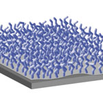
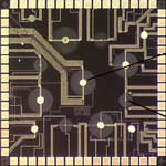 Gas sensors often operate by detecting the subtle changes that deposited gas molecules make in the way electricity moves through a surface layer. One advantage that carbon nanotubes offer for gas sensors, compared to metal oxide materials, is their fast response time and the fact that they react with gases at lower temperatures, sometimes even as low as room temperature. In order for CNT-based sensors to be able to compete with state-of-the-art CMOS technology, researchers need to develop a low cost, reliable and large-scale reproducible CNT deposition process on the wafer level. Researchers in the UK have now presented a novel concept of wafer level localized growth of 'spaghetti'-like CNTs on a fully processed CMOS substrate. This is the first successful proof of concept for growing CNTs at the post CMOS wafer stage.
Nov 15th, 2010
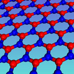 Along with graphene, boron nanoribbons have attracted more and more fundamental research interest. However, a major challenge in providing experimental evidence is that the preparation of atomically thin boron nanoribbons is very difficult. In new work that represents an important step in bridging theoretical predictions and experimental realization of atomically thin boron nanoribbons, reseaerchers demonstrate the successful fabrication of 'white graphene' nanoribbons - made of thermally and chemically stable atomic layers of hexagonal boron nitride - by unwrapping multiwalled boron nanotubes under delicate argon plasma etching. They show that the insulator-semiconductor electrical transition takes place during this processing and that this typically electrically insulating compound becomes a semiconductor when it is in ribbon morphology.
Nov 9th, 2010
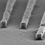
 Researchers at Harvard University have shown that nanostructures can be patterned with focused electron or ion beams in thin, stable, conformal films of water ice grown on silicon. They demonstrated ice lithography as a lithographic technique for patterning e.g. metal wires down to 20 nm wide. What's interesting about this technique is that patterning with ices of any condensed gas is a straightforward and practical process. Ice resist does not require spinning or baking. All processing and patterning steps can occur in a single evacuated chamber and be monitored at high resolution. The final removal of unexposed resist leaves minimal residues. Environmentally harmful solvents are not required and complete dry removal of the ice layer can be performed by in situ sublimation. Also, ice lithography makes it possible to nanopattern chemical modifications into silicon and other substrates. The team has now reported the successful application of ice lithography to the fabrication of nanoscale devices.
Nov 4th, 2010
 Many nanotechnology research projects require some form of nanopatterning technique in fabricating the devices, structures and surfaces required. With the current state of micro- and nanofabrication, the direct printing of functional materials is the most efficient method at low cost and low environmental impact. A direct printing approach has the merits of forgoing complex and expensive equipment, reducing the fabrication processes, saving the amount of material used, and removing chemical exposure in the processes. However, imprinting methods suffer from residues and difficulty in multi-alignment. Researchers in Korea have now developed a direct printing technique that is based on a liquid-bridge-mediated transfer moulding process.
Oct 20th, 2010
 In nature, uni- and multicellular organisms are capable of reducing and accumulating metal ions as detoxification and homeostasis mechanisms when exposed to metal ion solutions. Although the exact mechanisms and identities of microbial proteins associated for metal nanoparticle synthesis are not clear, two cysteine-rich, heavy metal-binding biomolecules, phytochelatin and metallothionein have been relatively well characterized. Phytochelatins are peptides that are synthesized by the protein phytochelatin synthase and that can form metal complexes with cadmium, copper, silver, lead and mercury, while metallothioneins are gene-encoded proteins capable of directly binding metals such as copper, cadmium, and zinc. This capability of phytochelatin and metallothionein - having different metal binding affinities to various metal ions - has now been employed by researchers for the in vivo biosynthesis of metal nanoparticles by recombinant Escherichia coli.
Sep 24th, 2010
 Nature can provide very useful templates for technical applications. A group of scientists have devised a new process involving the almost complete conversion of a leaf skeleton into magnetic iron carbide. To do this, they treated the leaf with iron acetate, nitrogen and heat. This technique can be used to recreate all natural carbonaceous structures with metal carbides. The result is not just beautiful, but also very useful. The new technique enables the conversion of metal carbides into intricate microstructures in just one step. Biology's intricate forms provide a wide range of templates for a variety of applications. Wide-ranging biological forms can be used as templates for filigree metal carbide structures using this method.
Sep 22nd, 2010
 Unlike most biological membranes, polymeric, nanometer-thin membranes are very stable and can withstand considerable pressure. This is an essential requirements for separation processes such as in water purification and desalination. Because their mechanical stability can be combined with flexibility and chemical functionality, polymer nanomembranes are also intensely researchers as materials for actuators and microsensors. They have also entered the biomedical field as artificial nacre and as a novel material used in surgery. Crosslinking of a spin-coated precursor solution, a common fabrication technique, reduces the interactions between the polymer chains and the environment and thus impairs the sensitivity and flexibility of the films. Researchers in Germany have now developed the first freestanding polymer brush, grafted from a crosslinked monolayer (nanosheet) that provides mechanical stability and structural integrity.
Sep 2nd, 2010
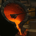 Along with control of fire, iron smelting is one of the founding technological pillars of civilization. Industry has used the same basic process to make iron for over 3000 years. Yet, it is also one of the major global sources of greenhouse gas release. Iron, a basic commodity, is still produced by the greenhouse gas intensive reduction of iron oxide by carbon-coke and currently accounts for the release of one quarter of worldwide carbon dioxide emissions by industry. For instance, on average 1.9 tonnes of carbon dioxide are emitted for every tonne of steel produced. Due to a large share of coal in the energy mix of current production technology, the CO2 emissions are high. Through a new understanding of the chemistry of iron at high temperature, researchers have uncovered an effective new carbon-dioxide-free process to form iron.
Aug 25th, 2010
 Subscribe to our Nanotechnology Spotlight feed