| Posted: Jul 08, 2014 | |
A universal and rapid method for transferring nanostructures |
|
| (Nanowerk Spotlight) Many nanofabrication techniques depend on creating a structure on one substrate and then transferring it via various processes onto another, desired, substrate. Nanoimprinting lithography (NIL) is such a pattern transfer process, as is poly(methyl methacrylate) (PMMA)-mediated peeling (see for instance "Free-standing nanosieve membranes that are only 1 nanometer thick"), or transfer printing with a polydimethylsiloxane (PDMS) stamp (for an example of this technique see: "Nanofabrication enables mass production of non-reflective polymer surfaces"). | |
| In the common PMMA-mediated transfer method, the etching of the supporting substrate to peel off PMMA/nanomaterial thin-film is usually carried out in hydrofluoric acid or hot potassium hydroxide solutions, which commonly requires more than 30 minutes processing time and is not environmentally friendly. | |
| "Many of these methods are not generally applicable as they suffer from the process-specific drawbacks, such as the requirement for the delicate control over the adhesion force at different interfaces, intolerance of transferred nanostructures to chemical etchant, and the harsh thermal environment needed for complete removal of polymer residues, as well as the wet-process-induced wrinkling of sheet structures," Hua Zhang, a professor in the School of Materials Science and Engineering at Nanyang Technological University (NTU), tells Nanowerk. "Defects resulting from these transfer processes often have dramatically hindered these devices' performance in electronic and optoelectronic devices." | |
| Zhang and his team have now proposed a universal and rapid method for transferring nanostructures with various dimensions – including zero-dimensional nanoparticles, one-dimensional nanowires, and two-dimensional (2D) nanosheets (graphene and transition metal dichalcogenide (TMD) nanosheets) as well as their hybrid structures from SiO2/Si substrates – onto diverse substrates with high fidelity. | |
| The team reported their findings in the June 23, 2014 online edition of ACS Nano ("A Universal, Rapid Method for Clean Transfer of Nanostructures onto Various Substrates"). | |
 |
|
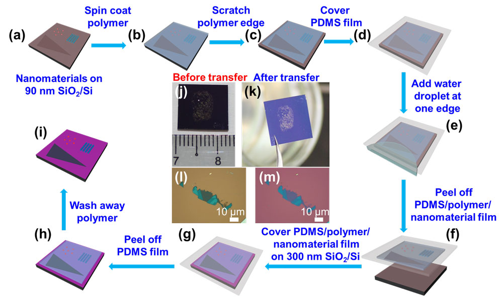
| Schematic illustration of high-fidelity transfer of nanostructures. (a) Low-dimensional nanomaterials (e.g., nanoparticle, nanowires, and nanosheets) are deposited on a 90 nm SiO2/Si substrate. (b) A polymer film as carrier is spin-coated onto the nanomaterials deposited on SiO2/Si substrate. (c) Polymer strips (1 mm wide) are removed at the edges of the polymer-coated SiO2/Si substrate to expose the hydrophilic SiO2 surface. (d) PDMS film (1-2 mm thick) is brought into conformal contact with the carrier polymer. (e) Drop of water is deposited at one edge of the SiO2/Si substrate to separate the PDMS/polymer/nanomaterial film from the SiO2/Si substrate. (f) PDMS/polymer/nanomaterial film is peeled off from SiO2/Si substrate. (g) PDMS/polymer/nanomaterial film is brought into contact with a 300 nm SiO2/Si substrate. (h) PDMS film is removed from the carrier polymer film. (i) Carrier polymer is washed away after it is dissolved in DCM at 50°C. The nanomaterials are left on the target substrate. (j) Photograph of MoS2 flakes deposited on a 90 nm SiO2/Si substrate. (k) Photograph of MoS2 flakes in (j) transferred onto a 300 nm SiO2/Si substrate. (l,m) OM images of the MoS2 nanosheets before (l) and after (m) transfer. (Reprinted by permission of American Chemical Society) (click on image to enlarge) | |
| Resembling more a 'cut and paste' operation, the whole transfer can be finished within several minutes. It also is compatible with temperature-sensitive materials and substrates because no thermal annealing is involved. | |
| In common transfer methods based on PMMA, thermal annealing is inevitable to remove the PMMA residue from transferred 2D nanosheets. By contrast, in Zhang's method, the carrier polymer can be completely removed in dichloromethane (DCM) at 50 °C, and achieve a surface cleanliness similar to that of thermal annealing. | |
| "Our method is suitable for a wide range of materials and substrates," Zhang points out the universal character of this new technique. "We demonstrated that various nanostructures can be successfully transferred onto diverse substrates, including hydrophilic (SiO2/Si), hydrophobic (octadecyltrichlorosilane modified SiO2), flexible (poly(ethylene terephthalate) film) substrates, and single crystals (BiFeO3, LiNbO3 and PMN-PT), with high fidelity. Not only hydrophobic nanosheets (graphene, MoS2 and WSe2), but also hydrophilic nanosheets (mica and graphene oxide) can be successfully transferred, indicating the wide applicability of our method." | |
| In summary, this transfer process exhibits three novelties: First, the peeling off process is assisted by water penetration at the interface of hydrophilic substrate and hydrophobic carrier polymer. It is clean and can be finished within several seconds. | |
| Second, the method is able to completely remove the carrier polymer without any annealing process, which greatly shortens the fabrication time required for the multi-step transfer. | |
| Finally, the carrier polymer is not limited to poly(L-lactic acid) (PLLA), poly(methyl methacrylate) (PMMA), and L-lactide-ε-caprolactone copolymer (PLC), which the team used in their present work. Any water insoluble polymer might be used for the rapid and clean transfer of nanomaterials. | |
| "The key advantages of our transfer method over previous techniques – i.e., rapidness, cleanness, and high precision – are especially important in the fabrication of vertically stacked heterostructures of graphene and other 2D nanosheets," says Zhang. "Previously, to make such vertical heterostructures, different 2D nanosheets were transferred layer by layer in sequence by using the common 'dry' transfer method based on PMMA. However, the PMMA residue cannot be completely removed even with high-temperature annealing. Impressively, our method is able to considerably remove the polymer residue in DCM without any annealing process, which greatly shortens the fabrication time required for the multistep transfer." | |
| Going forward, Zhang's team will try to improve their method for the transfer of large-area, CVD-grown TMD and topological insulator nanosheets from their growth substrates. Currently, the etching of copper foil is necessary prior to the transfer of CVD-grown graphene. | |
| "We will also try to transfer CVD-grown graphene on copper foil without etching the copper foil by using our method," he says. | |
 By
Michael
Berger
– Michael is author of three books by the Royal Society of Chemistry:
Nano-Society: Pushing the Boundaries of Technology,
Nanotechnology: The Future is Tiny, and
Nanoengineering: The Skills and Tools Making Technology Invisible
Copyright ©
Nanowerk LLC
By
Michael
Berger
– Michael is author of three books by the Royal Society of Chemistry:
Nano-Society: Pushing the Boundaries of Technology,
Nanotechnology: The Future is Tiny, and
Nanoengineering: The Skills and Tools Making Technology Invisible
Copyright ©
Nanowerk LLC
|
|
|
Become a Spotlight guest author! Join our large and growing group of guest contributors. Have you just published a scientific paper or have other exciting developments to share with the nanotechnology community? Here is how to publish on nanowerk.com. |
|