| Posted: Dec 28, 2007 | |
DNA electronics in nanotechnology |
|
| (Nanowerk Spotlight) DNA, the blueprint of life, and electronics seem to be two completely different things but it appears that DNA could offer a solution to many of the hurdles that need to be overcome in further scaling down electronic circuits beyond a certain point. The reason why DNA could be useful in nanotechnology for the design of electric circuits is the fact that it actually is the best nanowire in existence - it self-assembles, it self-replicates and it can adopt various states and conformations. | |
| Not surprisingly, performing reliable experiments on a single oligo-DNA molecule is an extremely delicate task as partly contradicting research reports demonstrate: Different DNA transport experiments have shown that DNA may be insulating, semiconducting, or metallic. Among the numerous factors that could impact the results are the quality of the DNA-electrode interface, the base pair, the charge injection into the molecule, or environmental effects such as humidity or temperature. | |
| Researchers have now demonstrated a novel carbon nanotube-based nanoelectronic platform as proof of concept that single DNA molecules can be detected. This novel detection technique is based on change in electrical conductance upon selective hybridization of the complementary target DNA with the single stranded probe attached to the system. The single-stranded sequence-specific probe DNA whose ends are modified with amine is attached between two carbon nanotubes/nanowires using dielectrophoresis (DEP). This platform can be used for understanding how electrical charge moves through DNA which could help researchers understand and perhaps develop a technique for reversing the damage of DNA done by oxidation and mutation. | |
| "We are able to use nanoscale electrodes to attach and measure electrical signals through single DNA molecule" Dr. Wonbong Choi explains to Nanowerk. "This is accomplished by suspending the DNA molecule in a nanoscale trench and chemically bonding them to the single wall carbon nanotube electrodes at its ends. Suspending the DNA between the electrodes eliminates the interaction of the molecule with the chip surface." | |
| Choi, an Associate Professor and Director of the Nanomaterials & Device Laboratory in the Department of Mechanical and Materials Engineering at Florida International University (FIU) in Miami, Florida, together with Dr. Kalai Mathee from FIU and collaborators from Pohang UniVersity of Science and Technology in South Korea, and National Institute of Genetics in Japan, also demonstrated the ability to use a single walled carbon nanotube, having the same diameter as a single double helix (∼ 2 nm) as an electrode to connect and measure electrical signals through the molecule. | |
| These findings, reported in a recent paper in Nano Letters ("Direct Electrical Measurements on Single-Molecule Genomic DNA Using Single-Walled Carbon Nanotubes"), are significant improvements over the electrical conductivity measurements of DNA demonstrated by other researchers. | |
 |
|
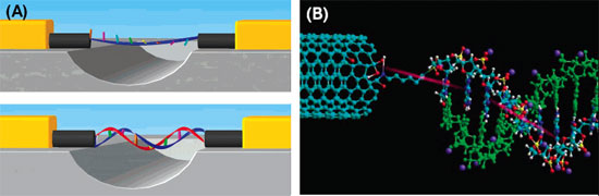
| Schematic illustrations. (A) The upper figure represents an arbitrarily shaped ssDNA molecule, which is stretched and attached to a pair of functionalized SWCNT electrodes in the presence of a DEP field. The lower figure depicts a covalently attached dsDNA molecule, which has a definite conformation. The nanoelectrodes are separated by a gap of 27±2 nm (the contour length of the 80 bp DNA molecule is ∼27 nm). The bridging DNA molecule suspends over a trench without touching the silicon dioxide surface. (B) Molecular diagram highlighting the covalent bonding between an amine-terminated ssDNA and a carboxyl-functionalized SWNT nanoelectrode via a (-CH2-)6 spacer. Charge transport takes place through the stacked base pairs in a helical duplex. (Reprinted with permission from American Chemical Society) | |
| "Typically, the diameter of the connecting leads is much larger than the size of the DNA molecule" says Choi. "Due to this, several DNA molecules are attached between connecting leads. Furthermore due to the dynamic material properties of the DNA molecule itself several other factors such as surrounding environment play a major role in studying electrical conductivity in DNA. For instance the interaction of DNA with the surface on which it is deposited completely changes the charge transport in DNA. All these factor have resulted in controversial results. In the development of our detection platform we are able to take into account all the above mentioned issues." | |
| The device fabrication itself is similar to what Choi and collaborators reported in previous work ("Transport Phenomena and Conduction Mechanism of Single-Walled Carbon Nanotubes (SWNTs) at Y- and Crossed-Junctions"). | |
| Choi explains that there are several unique aspects of his team's approach. "First, we have exploited single-walled carbon nanotube (SWCNT) electrodes for anchoring a DNA molecule of compatible diameter (1-2 nm). Second, the application of DEP in our system provides controlled manipulation of a DNA molecule. The third important issue is the formation of a covalent bond between each terminus of a DNA molecule and the functionalized end of a SWNT electrode. | |
| Establishment of a strong electronic coupling between the trapped molecule and the nanoelectrodes facilitates the charge transport through the system without the Coulomb blockade effect. The fourth important aspect is the presence of a nanotrench, between the SWCNT electrodes, that eliminates the contribution of the oxide surface to the charge transport through a DNA molecule. The suspended DNA molecule in our present system mitigates the problem of compression-induced perturbation of charge transport." | |
| The results of several control experiments confirmed that the measured electrical signals indeed originated from the anchored DNA molecules. | |
| One of the potential applications of the present study would be identification of specific genes based on the hybridization-induced change in electrical signal. The researchers explain that their current detection platform could be used in an application for the electrical detection of several other gene sequences on a single chip, although such simultaneous detection of several different gene sequences using an array of nanoelectrodes is a major challenge which currently is under investigation by the research team. | |
| This platform could also be used in fundamental research studies understanding the properties of DNA at single molecular level. The proposed technology has a wide-range application that includes but not limited to revealing the presence of disease related genes, bacterial and viral. | |
 By
Michael
Berger
– Michael is author of three books by the Royal Society of Chemistry:
Nano-Society: Pushing the Boundaries of Technology,
Nanotechnology: The Future is Tiny, and
Nanoengineering: The Skills and Tools Making Technology Invisible
Copyright ©
Nanowerk LLC
By
Michael
Berger
– Michael is author of three books by the Royal Society of Chemistry:
Nano-Society: Pushing the Boundaries of Technology,
Nanotechnology: The Future is Tiny, and
Nanoengineering: The Skills and Tools Making Technology Invisible
Copyright ©
Nanowerk LLC
|
|
|
Become a Spotlight guest author! Join our large and growing group of guest contributors. Have you just published a scientific paper or have other exciting developments to share with the nanotechnology community? Here is how to publish on nanowerk.com. |
|