| Posted: Jan 27, 2017 | |
Computational and patterning approaches to realize metasurfaces in novel plasmonic materials |
|
| (Nanowerk Spotlight) Compact optical components are crucial to realize miniaturized optical systems and integrated optoelectronic devices. Plasmonic metasurfaces – structured materials in 2D with rationally designed, subwavelength-scale building blocks – have drawn great interest because they can control light based on subwavelength structures. These planar devices are attractive for applications ranging from high resolution imaging to 3D holography. | |
| Recent work has further shown that metasurfaces with a thickness below 200 nm can achieve efficient polarization control and ultrasensitive biosensing. | |
| Integrated optoelectronic devices based on metasurfaces, however, is challenging to achieve because traditional plasmonic materials including silver and gold are not compatible with current semiconducting processing. | |
| Recently, titanium nitride (TiN) has received attention as an unconventional plasmonic material because of its potential CMOS (complementary metal-oxide-semiconductor) compatibility as well as exceptional mechanical strength and high-temperature stability required for operation in extreme conditions. | |
| Despite tremendous interest, experimental demonstration of TiN metasurfaces has not been reported. One major challenge is that traditional metasurface designs require stringent accuracy in fabrication while patterning TiN nanostructures precisely is extremely difficult. | |
| New work by the Odom Group at Northwestern University describes the design and prototyping of single-crystalline TiN plasmonic metasurfaces based on subwavelength hole arrays. The results have been published in ACS Photonics ("Evolutionary Design and Prototyping of Single Crystalline Titanium Nitride Lattice Optics"). | |
 |
|
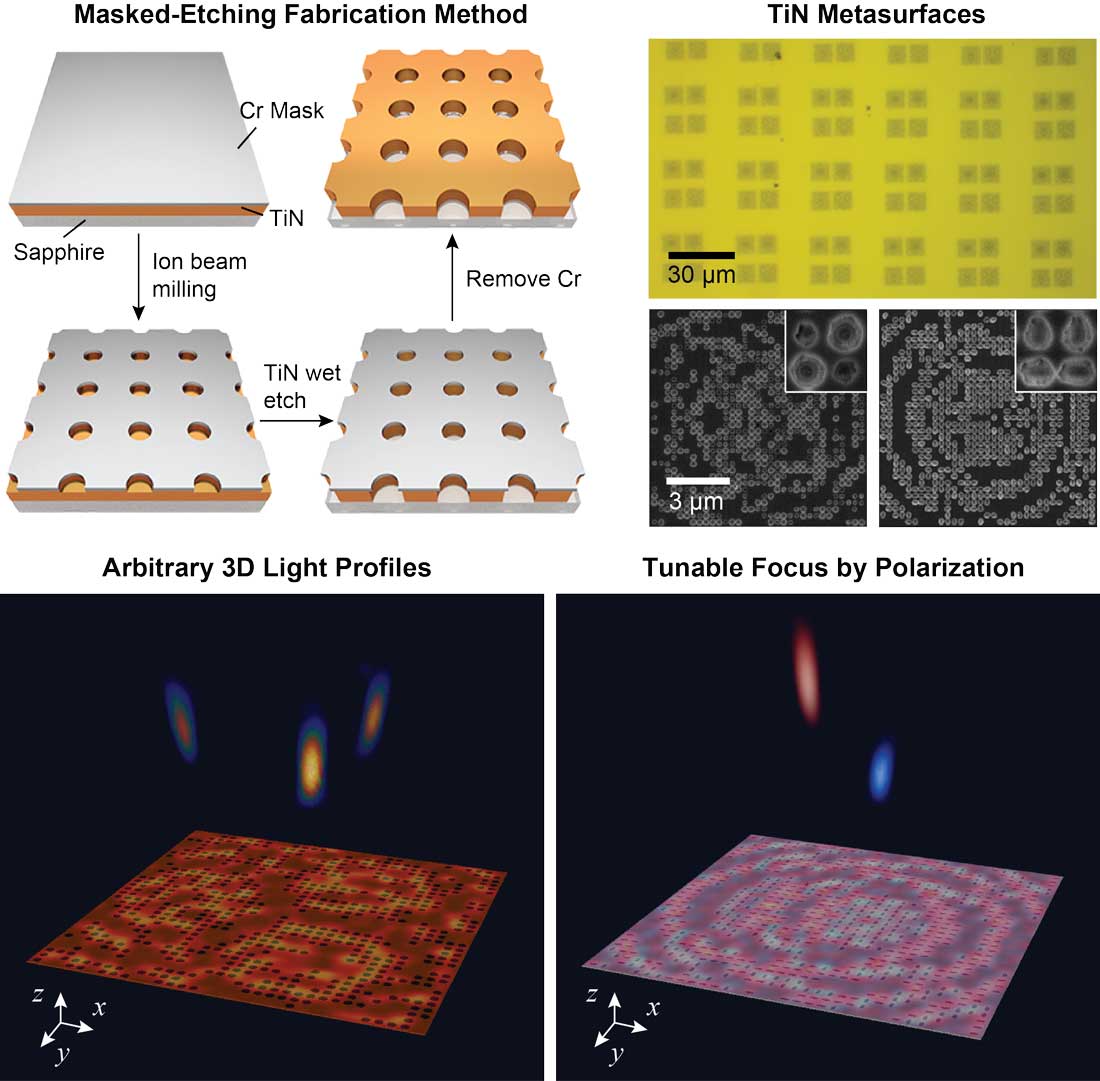
| The masked-etching technique can rapidly prototype TiN metasurfaces designed by our evolutionary algorithm over large area with control over nanohole size and shape. Because evolutionary algorithms allowed efficient multi-objective optimization, lattice structures could be designed to focus light simultaneously to multiple light spots with arbitrary 3D arrangements. The metasurfaces also achieved dynamic tuning of far-field responses by using anisotropic nanoholes as building units. (Image: Jingtian Hu, Odom Group, Northwestern University) (click on image to enlarge) | |
| "We developed an evolutionary algorithm to design plasmonic metasurfaces and an associated prototyping method for single-crystalline TiN films," Teri W. Odom, Charles E. and Emma H. Morrison Professor of Chemistry and Professor of Materials Science and Engineering at Northwestern University, tells Nanowerk. "Implemented under the object-oriented paradigm, the versatile, black-box design program was highly customizable and user-friendly." | |
| The algorithm employed a novel objective function that can achieve multi-spot focusing, where both the optical patterns and focal intensity can be tuned accurately. The sizes and shapes of nanoholes can be tailored to achieve multiphase TiN metasurfaces. | |
| Previously, Odom's team has reported a lattice evolution algorithm (LEA) as an efficient approach to design nanohole metasurfaces in a gold film (see our Nanowerk Spotlight on this: "Ultra-thin achromatic lenses optimized by an evolutionary algorithm"). In that work, the researchers developed a highly efficient, universal algorithmic method based on evolutionary principles for the design of ultra-thin achromatic lenses. | |
| The team's new work features an object-oriented lattice evolution algorithm (OLEA) and a parallel patterning process to prototype designs. | |
| Using anisotropic nanohole shapes, the team demonstrated dynamic tuning of the optical responses by changing the polarization state of incident light. | |
| "The optimize-and-prototype platform we established here can contribute to expanding metasurface designs to a wide range of applications requiring unconventional materials systems," notes Odom. " This might be of great interest to the computational materials science community interested in developing efficient design methods for structured metamaterials." | |
| This platform could also be used in fast, versatile patterning techniques for prototyping nanostructures on unconventional materials. Finally, the nanophotonics community interested in achieving compact, micro-optics systems for high-temperature operations could put this new prototyping technique to good use. | |
 By
Michael
Berger
– Michael is author of three books by the Royal Society of Chemistry:
Nano-Society: Pushing the Boundaries of Technology,
Nanotechnology: The Future is Tiny, and
Nanoengineering: The Skills and Tools Making Technology Invisible
Copyright ©
Nanowerk LLC
By
Michael
Berger
– Michael is author of three books by the Royal Society of Chemistry:
Nano-Society: Pushing the Boundaries of Technology,
Nanotechnology: The Future is Tiny, and
Nanoengineering: The Skills and Tools Making Technology Invisible
Copyright ©
Nanowerk LLC
|
|
|
Become a Spotlight guest author! Join our large and growing group of guest contributors. Have you just published a scientific paper or have other exciting developments to share with the nanotechnology community? Here is how to publish on nanowerk.com. |
|