Showing Spotlights 89 - 96 of 625 in category All (newest first):
 Researchers have developed an antiviral dressing material with visible-light-activated sterilizing properties that enables physical and chemical protection against viral agents like Herpes simplex. They re-engineered a common additive agent found in sunscreen (zinc oxide) to be self-sterilizing within a non-woven fibrous mats for herpes virus treatment. The self-sterilizing function creates a 'green' associated oxidant hydrogen peroxide (hydrogen peroxide), capable of eliminating harmful bacteria and viruses.
Oct 12th, 2021
 Polymer dielectrics are widely used as an insulating material in advanced electronics and electric power systems that require operation at high temperatures and high breakdown conditions. The miniaturization and higher power of modern electronics generate lots of heat, which needs to be dissipated quickly to avoid device malfunction or breakdown. This increased heat also leads to the temperature rise of insulating materials, which gradually causes the loss of dielectric performance. To address this, researchers report a new strategy to achieve high thermal conductive electric insulator polyethylene with high dielectric constant and strength.
Sep 30th, 2021
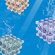 Hydrogels are fascinating natural or synthetic polymer materials that exhibit very versatile chemistries and physical or biological properties. They are 3D networks of either physically or chemically crosslinked polymers that resemble organic tissues and that can hold large amounts of water within their interlocked molecular network. These soft, translucent materials swell or shrink in response to water absorption or desorption and can hold a large amount of water without losing their structural integrity.
Aug 30th, 2021
 The bottleneck in atomic-scale data storage area may be broken by a simple technique, thanks to recent innovative studies. Through a simple, efficient and low-cost technique involving the focused laser beam and ozone treatment, researchers can manipulate the properties of nanomaterials, thereby 'writing' information onto monolayer materials. The result is a demonstration of the thinnest light disk with rewritable data storage and encryption functionalities at the atomic level.
Jul 28th, 2021
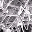
 Scientists have discovered a new class of material which, when fractured, can repair themselves within milliseconds. The highly crystalline materials, when broken into pieces, can self-propel and re-join in the blink of an eye, and repair themselves so precisely that they become indistinguishable from the undisturbed materials. These new materials may find applications in various high-tech applications. During repair, fractured pieces travel with a honeybee wing-like motion with acceleration comparable to cars.
Jul 26th, 2021
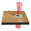 Optical tweezers used to trap nanoscale objects usually require a tightly focused laser beam with high optical intensity. The problem with all conventional laser-based optical manipulation techniques is that the laser light could cause photodamages and photothermal degradation to nanoparticles and biological samples. A novel solution to this problem creates a low-temperature spot in the solution and trap particles and molecules at the cold spot. This new technique can effectively avoid photothermal damages.
Jun 29th, 2021
 Scientists have created a new way to monitor subtle drug interactions between bacteria and antibiotics. By using a common office inkjet printer, researchers developed a disposable living laser on chip by encapsulating living bacteria inside. Strong laser emissions generated from bacteria inside the droplet will be dramatically enhanced during drug interactions. This breakthrough could enable more sensitive and high-throughput testing using micro-nano laser technology in the near future.
Mar 25th, 2021
 The properties ofvan der Waals heterostructures can be precisely controlled by twisting the stacked atomic layers, opening the way for the use of this unique degree of freedom for the nanoscale control of composite materials and nano-devices in future technologies. New work suggests that all 2D materials could also be rolled into their 1D counterparts and a plethora of function-designable 1D heterostructures could be realized. Unlike semiconductor nanowires or mono-elemental nanotubes, which are rolls of one type of material, these novel nanostructures would have very different, and customizable, properties.
Mar 2nd, 2021
 Subscribe to our Nanotechnology Spotlight feed