Showing Spotlights 1233 - 1240 of 2798 in category All (newest first):
 Fabrication of three-dimensional (3D) objects through direct deposition of functional materials - also called additive manufacturing - has been a subject of intense study in the area of macroscale manufacturing for several decades. These 3D printing techniques are reaching a stage where desired products and structures can be made independent of the complexity of their shapes. Researchers in Korea have now shown that nanoscale 3D objects such as free-standing nanowalls can by constructed by an additive manufacturing scheme.
Feb 5th, 2014
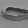
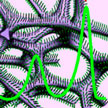
 Over the years, researchers have developed a large number of techniques to synthesize nanowires and nanotubes in the laboratory. These procedures vary widely in their hardware requirements and methodology. Nevertheless, they all share a set of common goals: simplicity of protocol; fast execution; and low energy input. Now, an international group of scientists has reported a breakthrough in all three of these areas, leading to a revolutionary and remarkably simple technique for preparing one-dimensional nanostructures. As an example, they demonstrate a unique approach to growing amorphous boron nanowires.
Feb 4th, 2014
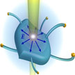
 Ingenuity Lab in Edmonton, Alberta are taking cues from nature, as they focus on nanotechnology gains in the area of biomining. Using microorganisms and biomolecules, the group is making significant advances in the recovery of rare earth and precious metals from industrial processes and the environment thanks to superior molecular recognition techniques. The researchers at Alberta's first nanotechnology accelerator laboratory are looking to take advantage of inorganic binding peptides for mining valuable and rare earth elements/metals that exist in nature or synthetic materials.
Feb 3rd, 2014
 Nanowire field-effect sensors show significant advantages of real-time, label-free and highly sensitive detection of a wide range of analytes in liquid phase, including proteins, nucleic acids, small molecules, and viruses in single-element or multiplexed formats. Motivated by the unique features of these sensors and the ease to integrate them in the currently available VLSI technology, researchers used molecularly modified silicon nanowire FETs to detect volatile organic compounds (VOCs) that are associated with environmental pollution, quality control, explosive materials, or various diseases.
Jan 30th, 2014
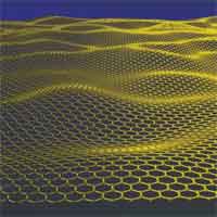 Graphene is undoubtedly emerging as one of the most promising nanomaterials because of its unique combination of superb properties, which opens a way for its exploitation in a wide spectrum of applications ranging from electronics to optics, sensors, and biodevices. In this Nanowerk nanotechnology primer we summarize recent finding in graphene research and show the breadth of graphene applications in such areas as energy, electronics, sensors and many others.
Jan 29th, 2014
 Recently, nanotechnology researchers have begun to work with graphene foams - three-dimensional structures of interconnected graphene sheets with extremely high conductivity. Since graphene foam possesses a high porosity of close to 100%, this offers the opportunity to use it as a scaffold for other nanomaterials to generate synergistic effects. Now, researchers have fabricated vertically aligned ZnO nanowire arrays on 3D graphene foam and used this electrode to detect uric acid in a reliable statistical level from the serum of Parkinson's disease patients.
Jan 27th, 2014
 Paper could lead to low-cost innovative devices and applications is lab-on-a-chip technology. In new work, researchers in Korea have, for the first time, used paper as a platform material for actively actuating an electronic microfluidic chip. This novel, powered fluidic chip - known as an active paper open chip (APOC) - allows the full range of fluidic operations by implementing an electric input on paper via an electrowetting technique.
Jan 23rd, 2014
 Transparent and flexible substrates are widely explored for flexible electronics and researchers have been working on techniques to develop thermally stable and biodegradable materials that are as easily printable as paper. Previously, we reported on a transparent and flexible nanopaper transistor. The same team has now reported a novel transparent paper substrate design optimized for solar cells. They introduced a novel transparent paper made of earth-abundant wood fibers that simultaneously achieves an ultrahigh transmittance and ultrahigh optical haze.
Jan 22nd, 2014
 Subscribe to our Nanotechnology Spotlight feed