Showing Spotlights 161 - 168 of 338 in category All (newest first):
 Although graphene properties and applications have already been well-discussed in the literature, it also is important to understand how 2D chemistry of graphene and graphene analogs is related to various applications. Graphene functionalization modifies the unique 2D features of graphene. In this way, the electronic and physical properties of graphene can be controlled toward the given purpose such as highly effective novel electronic device applications. Already, graphene functionalization such as adsorption, intercalation, and doping toward device applications has attracted great attention.
Aug 10th, 2017
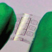
 Researchers have developed a stretchable and transparent graphene-based electronic tattoo (GET) sensor that is only hundreds of nanometers thick but demonstrates high electrical and mechanical performance. They show that a GET can be fabricated through a simple wet-transfer/dry-patterning process directly on tattoo paper, allowing it to be transferred on human skin exactly like a temporary tattoo, except this sensor is transparent. Due to its ultra-thinness, a GET can fully conform to the microscopic morphology of human skin via just van der Waals interactions and can follow arbitrary skin deformation without mechanical failure or delamination for an extended period of time.
Jul 31st, 2017
 Graphene currently is the most studied material on the planet - this is especially true for charge storage and the results from many laboratories confirm its potential to change today's energy-storage landscape. Specifically, graphene could present several new features for energy-storage devices, such as smaller capacitors, completely flexible and even rollable energy-storage devices, transparent batteries, and high-capacity and fast-charging devices.
Jul 20th, 2017
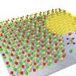 The ultimate challenge of nanotechnology is to control the structure of matter with atomic precision. The better we are at shaping and structuring material on a small scale, the more powerful technology we can dream of. Unfortunately, the atomic scale is entirely out of range for conventional patterning. Researchers now report that they have achieved nanoscale self-assembly within a two-dimensional layer. Dosing of ethylene and borazine near a hot iridium surface, leads for self-organising of a two-dimensional superlattice of graphene dots.
Jun 29th, 2017
 As two-dimensional (2D) materials gain more and more importance - thanks to their exotic electronic properties and abundant active sites - the development of high-yield, efficient, fast and low-cost synthesis methods to advance these materials from the laboratory to industry has become an urgent issue. Now, researchers have developed a general and rapid molten salts method that can synthesize various ion-intercalated 2D metal oxides and hydroxides, such as cation-intercalated manganese oxides, cation-intercalated tungsten oxides, and anion-intercalated metal hydroxides.
Jun 23rd, 2017
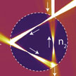 Modern-day electronics or communication technology would not exist without electron microscopy, and the same can be said for many other types of technology. Beyond imaging, the focused beam of electrons is also used for analysis of the chemical composition, the crystal structure, and many other useful things. In new work, researchers have proposed to use graphene as a two-dimensional vacuum chamber, and build a two-dimensional electron microscope, where the electrons fly from the electron gun to the target without ever leaving the graphene sheet.
Jun 9th, 2017
 Inspired by the unique optical and electronic property of graphene, two-dimensional layered materials - as well as their hybrids - have been intensively investigated in recent years, driven by their potential applications for nanoelectronics. The broad spectrum of atomic layered crystals includes transition metal dichalcogenides (TMDs), semiconducting dichalcogenides, monoatomic buckled crystals, such as black phosphorous (BP), and diatomic hexagonal boron nitride, etc. Tihis article examines the recent advancement of flexible 2D electronic devices based on TMDs and BP.
May 23rd, 2017
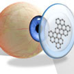 Several research projects are working on reinventing the contact lens as a smart electronic device that, for instance, works as a self-powered biosensor for various point-of-care monitoring and wireless biomedical sensing. n addition to sensors, researchers are devising numerous applications for smart contact lenses, ranging from drug delivery systems to protection from electromagnetic wave damage. An application closer to contact lenses' original function, graphene can change the focal length of a polymeric soft contact lens in order to adjust near- and farsightedness.
May 22nd, 2017
 Subscribe to our Nanotechnology Spotlight feed