Showing Spotlights 145 - 152 of 338 in category All (newest first):
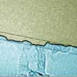
 Single- or few-layer black phosphorus (BP) is one of the most promising two-dimensional semiconductors for electronic and optoelectronic device applications but its environmental instability has always posed a major hurdle for BP-based devices. In contrast, black phosphorus analogues (BPA) nanoarchitectures not only own the similar folded structure of BP, its tunable bandgap energy band and high carrier mobility, but exhibit excellent environmental stability as well. BPA nanosheets can be fabricated by a facile liquid-phase exfoliation method.
Mar 14th, 2018
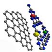
 Due to its fascinating properties, black phosphorus (BP) has demonstrated appealing potential for not only building (opto)electronic devices, but also in many other areas such as lithium-ion batteries, solar cells, sensors, thermoelectric devices, supercapacitors, and phototherapy. Researchers now have demonstrated that modifying BP with metal ions solved its previous instability problem, which hindered the practical application of BP in electronics and optoelectronics; while at the same time further enhancing the original superior transport properties.
Mar 7th, 2018
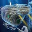
 For the first time, liquid-phase exfoliation (LPE) - a widely explored technique to obtain two-dimensional (2D) layered nano-architectures - has been successfully used to exfoliate tellurium, a non-layered material. The resulting 2D Te nanosheets exhibit excellent photoresponse behavior from the UV to the visible regime in association with strong time and cycle stability for on/off switching behavior. This intriguing finding could help in the search for other 2D materials for innovative applications.
Mar 5th, 2018
 Recently, a new member has been introduced to the family of two-dimensional (2D) materials: phosphorene. Phosphorene has attracted much attention because of its tunable direct band gap and superior carrier mobility, but unfortunately phosphorene is subjected to oxidation and degradation under ambient conditions. Now, researchers have reported a facile pathway in obtaining and stabilizing phosphorene through a one-step, ionic liquid-assisted electrochemical exfoliation and synchronous fluorination process. This strategy enabled a novel phosphorene derivative to be discovered - fluorinated phosphorene, which exhibits air-stable photo-thermal properties.
Mar 2nd, 2018
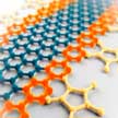 Scientists report a systematic study involving theoretical and experimental approaches to evaluate the Li-ion storage capability in 2D atomic sheets of nonlayered MoO2. They describe a new process - polymer-assisted reduction - to make atomically flat 2D sheets of MoO2. Since MoO2 is not a 2D material, this process opens a new pathway to make 2D nanostructures from non-layered materials. By successfully making 2D atomic sheets of MoO2, the researchers fabricated a battery electrode in which the Li ion diffusion and electron transport are exceptionally fast.
Feb 15th, 2018
 Researchers have looked closer at the Hall effect in narrow graphene devices - so-called graphene nanoribbons and nanoconstrictions. They were puzzled when they found that the quantization of the conductance was destroyed in some samples - especially because these particular samples were optimized for low edge disorder and low contamination. As it turned out, this effect had been predicted by several theoretical physicists twenty years ago, but largely ignored since no experimental evidence was ever found.
Feb 13th, 2018
 Optics and mesoscopic physics teams have discovered a new cooling mechanism concerning electronic components made of graphene deposited on boron nitride. The efficiency of this mechanism allowed them to reach electric intensities at the intrinsic limit of the laws of conduction. This new mechanism, which exploits the two-dimensional nature of the materials opens a 'thermal bridge' between the graphene sheet and the substrate. Researchers have demonstrated the effectiveness of this mechanism by imposing in graphene levels of electrical current still unexplored, up to the intrinsic limit of the material and without any degradation of the device.
Jan 9th, 2018
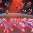
 Efficient electrocatalysts lie at the heart of a series of significant energy conversion and storage technologies, and atomically precise understanding of the influences of component dopants is crucial for looking into the reaction mechanism and controlled synthesis of the desired electrocatalysts. Graphitic carbon nitride is a promising electrocatalytic material owing to its intrinsically high N content and abundant edge sites. This material has been researched towards some of the most significant electrocatalytic reactions including oxygen reduction/evolution reaction and hydro evolution reaction. New work has comprehensively explored the influences of component elements within graphitic carbon nitride motiety for electrocatalytic reactions.
Nov 13th, 2017
 Subscribe to our Nanotechnology Spotlight feed